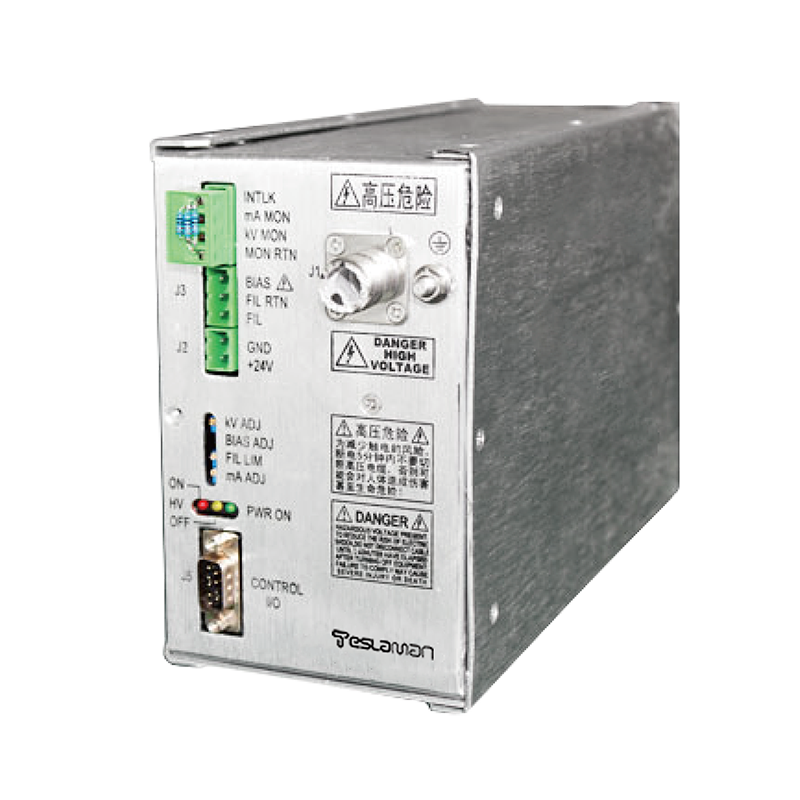
Technical Requirements for High-Voltage Power Supplies in Electronics Manufacturing
In the precision processing system of electronics manufacturing, high-voltage power supplies (HVPS) serve as critical energy regulation units, whose output characteristics directly affect the precision and yield of semiconductor wafer fabrication, printed circuit board (PCB) processing, and display panel production. Given the nanometer-level process control and complex electromagnetic environments involved, HVPS must meet multi-dimensional technical specifications to enable precise control of core processes such as material etching, ion implantation, and plasma excitation. This article analyzes the key technical requirements and engineering implementation paths of HVPS from typical manufacturing scenarios.
1. High-Precision Energy Supply for Semiconductor Wafer Fabrication
In the front-end semiconductor process, HVPS are mainly used in ion implanters and plasma etching equipment, requiring three highs and one stability:
1. High-Voltage Output Accuracy: Ion implantation requires 10-300kV DC high voltage to accelerate impurity ions, with voltage stability reaching ±0.01% (24-hour drift <0.05%) to ensure ion energy distribution deviation <0.1%, avoiding device performance dispersion caused by uneven wafer doping concentration.
2. Ripple Suppression Capability: The RF matching network of plasma etching machines relies on HVPS drive, requiring the DC bus voltage ripple coefficient to be controlled below 0.05% (peak-peak <50mV) to prevent ripple noise from causing plasma density fluctuations and affecting etching linewidth precision (target ±5nm).
3. Dynamic Response Speed: Facing changes in wafer surface topography (e.g., deep trench etching), the power supply must have a μs-level response speed, compensating for plasma impedance changes through real-time high-voltage adjustment to control etching rate fluctuations within ±2%.
4. Electromagnetic Compatibility (EMC): A three-stage filtering architecture (common-mode inductor + differential-mode capacitor + shielded cavity) ensures conducted interference <40dBμV in the 150kHz-30MHz band and radiated interference <30dBμV/m (30-1000MHz), avoiding signal acquisition interference with wafer inspection equipment.
2. Electrochemical Process Adaptation in PCB Processing
In wet processes such as PCB electroplating, electroless copper plating, and via etching, the technical requirements of HVPS are deeply coupled with material electrochemical properties:
Pulse Waveform Customization: Hard gold plating requires bidirectional pulses of 1-50kHz (forward voltage 5-15V, reverse voltage 1-3V). The power supply must support continuous adjustment of pulse width duty cycle (0.1%-99.9%) with a positive/negative pulse switching time <1μs, ensuring fine plating crystallization (roughness Ra <0.2μm).
Low-Noise Grounding Design: Suspended grounding and multi-point shielding technology control the potential difference between the power supply ground and production equipment ground below 10mV, preventing electrochemical parameter drift of the plating solution caused by ground loop currents and ensuring via resistance uniformity in through-hole metallization (target deviation <3%).
Insulation Reliability: For acidic/alkaline electrolyte environments, the power supply housing must pass IP67 protection testing, and internal high-voltage modules use nano-coating insulation (volume resistivity >10¹⁴Ω·cm) to ensure leakage current <10μA in 95% humidity, avoiding power failures due to electrochemical corrosion.
3. Plasma Regulation Technology for Display Panel Production
In the array manufacturing and bonding processes of LCD/OLED panels, HVPS must meet dual requirements for plasma uniformity and process safety:
1. Uniform Electric Field Generation: Plasma cleaning requires an electric field strength deviation <1.5% in a 300mm×400mm effective area. The power supply drives arrayed electrodes through multi-channel synchronization technology (phase difference <0.1°), combined with voltage feedback compensation algorithms, to control discharge current fluctuations within ±1%.
2. Rapid Overcurrent Protection: Facing film short-circuit risks at panel edges, the power supply must have 50ns-level short-circuit detection capability with a trigger response time <1μs. Using current-limiting resistors and solid-state relays, fault energy is limited to <50mJ to avoid permanent substrate damage from plasma discharge.
3. Wide-Temperature Operation Adaptability: In low-temperature processes (-20℃), internal capacitors use tantalum polymer dielectrics (operating temperature range -55℃~+125℃). With intelligent heating modules, the output voltage build-up time during startup is <200ms, meeting the production line's continuous operation cycle requirement (UPH≥150).
4. Common Technical Requirements and Engineering Challenges
Beyond scenario-specific needs, electronics manufacturing imposes three common technical specifications on HVPS:
1. Safety Compliance: Must pass IEC 61010-1 double insulation certification, with active discharge function at the high-voltage output (residual voltage <60V DC, discharge time <10s) to prevent electric shock risks for maintenance personnel.
2. Intelligent Interaction: Integrated with RS-485/Ethernet interfaces supporting Modbus TCP protocol, real-time uploading voltage/current/temperature data (sampling frequency 1kHz) and receiving remote parameter configuration from the host computer (resolution 0.1% of rated value).
3. Thermal Management Efficiency: Combining micro-channel liquid cooling (channel size 0.3mm) with phase-change heat dissipation keeps the power module junction temperature below 85℃ (at 40℃ ambient temperature), ensuring a service life >100,000 hours (MTBF >50,000 hours) under 24/7 operation.
Current technical challenges focus on high-frequency noise suppression (interference above 10MHz) and power density improvement (target >20W/in³), requiring integrated magnetic component design and silicon carbide (SiC) device applications to meet Class B EMC standards while reducing size.
5. Future Development Trends
With the popularization of advanced processes such as Mini-LED and 3D packaging, HVPS will evolve toward:
Nanometer-Level Precision Control: Developing sub-millivolt voltage regulation technology (resolution 0.1mV) to adapt to ultra-precision processes like atomic layer deposition (ALD).
Multi-Field Coupling Collaboration: Integrating high-voltage, RF, and pulsed magnetic field multi-energy outputs to support plasma-thermal-force multi-physical field coupling processing, expanding applications in flexible electronics manufacturing.
Self-Diagnostic Intelligence: Embedded AI algorithms analyze discharge waveform characteristics in real time, predicting insulation aging (accuracy >95%) and enabling a shift from preventive to predictive maintenance.