


Electron beam exposure machine Recommended Products
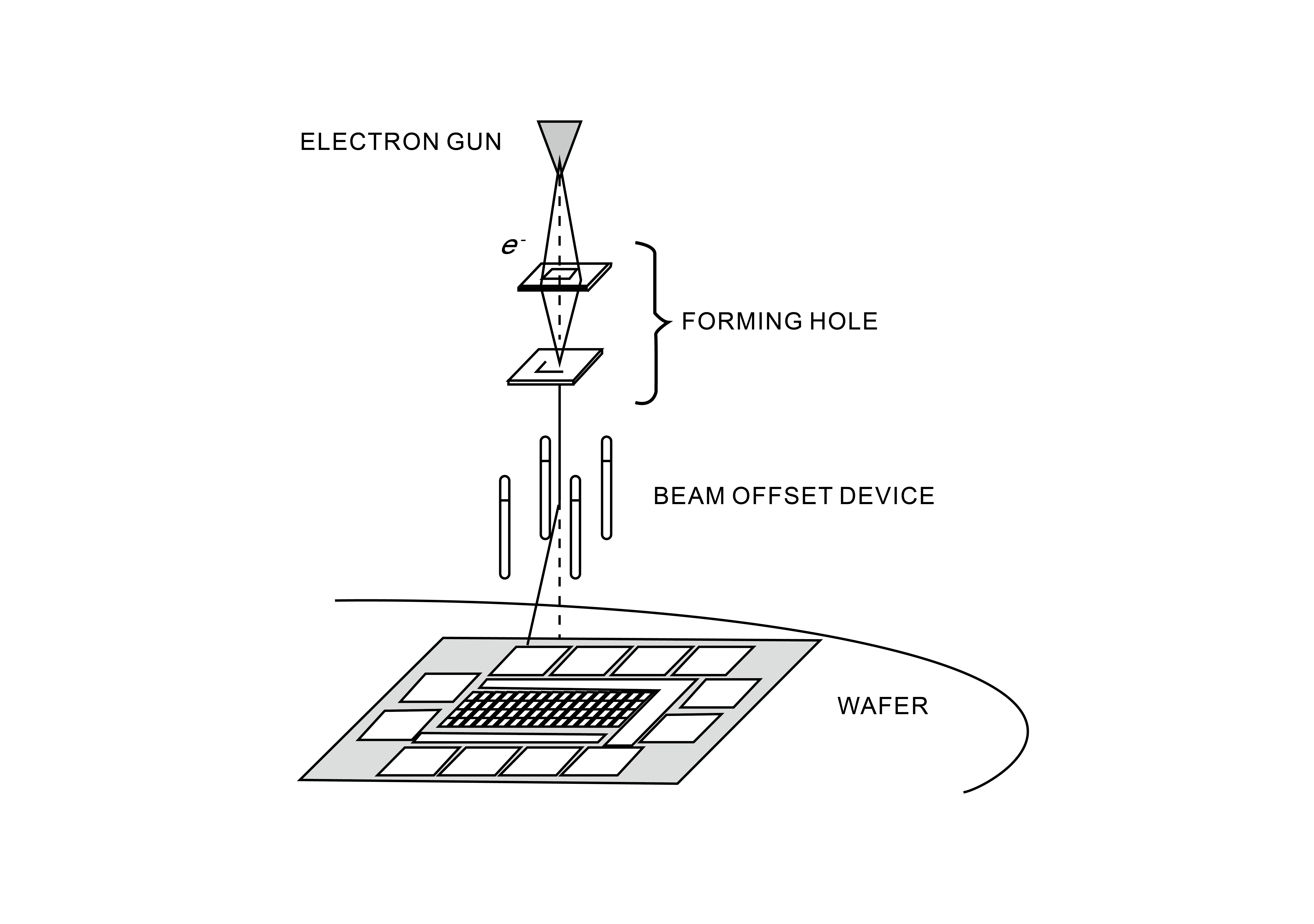
Electron beam exposure machine
It is mainly used in the fields of semiconductors, nanotechnology and materials science. Besides its wide application in the semiconductor integrated circuit field, typical applications of electron beam lithography in the instrument field include: extreme ultraviolet and X-ray focusing/imaging/spectroscopic components, standard samples and test cards for instrument testing and calibration at a scale of less than 100nm, extremely high working frequency surface acoustic wave transducers, planar lens components for the next-generation optical system, and third-generation nanopore DNA sequencing, etc.