


Transmission electron microscope
Extremely low ripple and ultra-stable output (1ppm level) High voltage output and wide modulation range (0-400kV) High reliability and long service life Intelligent and digital control Highly customized solutions can be provided
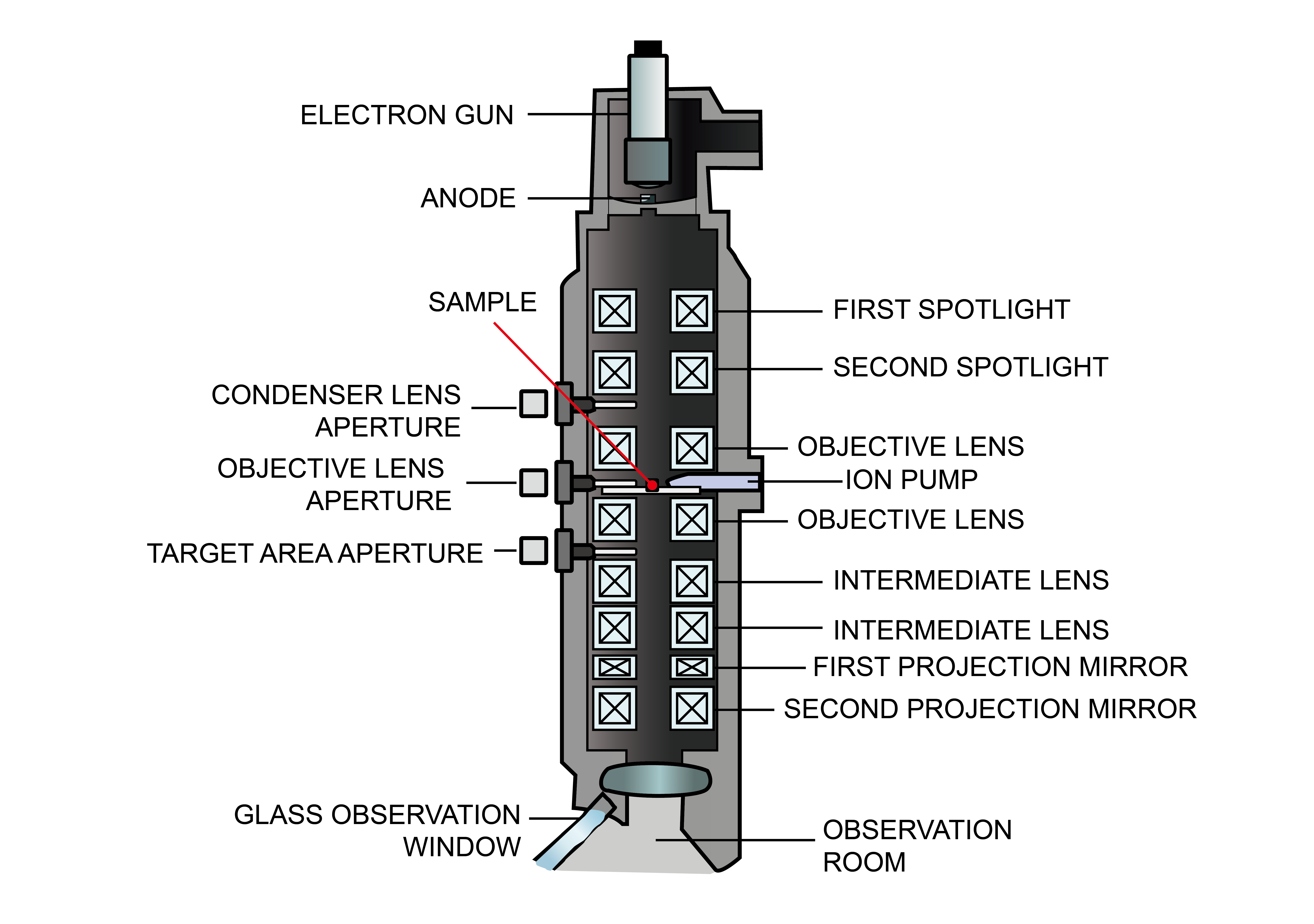
Transmission electron microscopy (TEM) utilizes an accelerated electron beam to penetrate ultrathin samples, forming images through the difference in scattering angles caused by the collision of electrons and atoms. With a resolution of 0.1 to 0.2nm and magnification ranging from tens of thousands to millions of times, it is widely used in the observation of ultra-microstructures. In the semiconductor field, it is mainly applied to the crystal structure analysis of semiconductor materials, the structural characterization of semiconductor devices, the doping distribution and diffusion of semiconductor materials, the failure analysis of semiconductor devices, and the structural optimization in semiconductor manufacturing processes, etc.