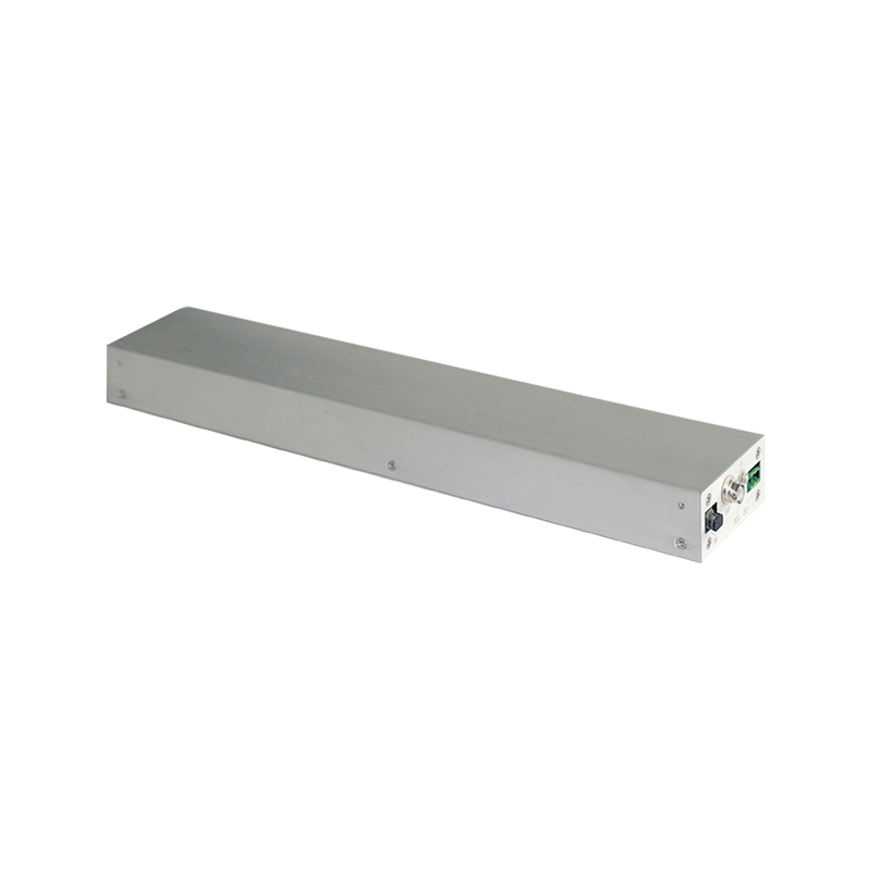
High-voltage Power Supply Precision Innovation for PCB Testing: Application Breakthroughs
1. Evolution of Power Supply Precision Requirements in PCB Testing
In the field of printed circuit board (PCB) manufacturing, the demand for power supply precision in the testing phase has upgraded from traditional functional testing to micron-level defect localization. With the popularization of high-density interconnect (HDI) technology, the line width of PCBs has been reduced to less than 50μm. In scenarios such as insulation breakdown voltage testing and impedance continuity detection, the stability of power supply output directly affects the reliability of test results. Although traditional linear power supplies have low ripple characteristics, their response speed lags behind high-frequency detection signals, while the topology of switching power supplies is susceptible to electromagnetic interference (EMI) under high-frequency conditions, causing voltage fluctuations exceeding ±1%FS (full scale), which is difficult to meet the multi-layer interconnection detection requirements of advanced PCBs.
2. Core Breakthrough Directions of Technological Innovation
1. Reconstruction of Closed-loop Control Driven by Digital Twin
New high-voltage power supplies introduce digital twin technology to build a virtual mapping of the power supply model and PCB load in the FPGA controller. Based on finite element analysis (FEA), the model real-time calculates the influence of parasitic parameters, compressing the traditional PID control cycle from 100μs to less than 20μs. For example, in a 10kV output scenario, the adaptive Kalman filter algorithm can dynamically compensate for voltage caused by load changes, improving the steady-state precision to ±0.1%FS and shortening the transient response time to less than 50μs, meeting the transient high-voltage requirements for blind via plating defect detection.
2. Topological Innovation of Wide-bandgap Semiconductors
The application of third-generation semiconductor devices (such as silicon carbide SiC MOSFET) promotes the upgrading of power supply topology to LLC resonant structure. Compared with the traditional IGBT scheme, the switching loss of SiC devices at a switching frequency of 100kHz is reduced by 60%. With a multi-stage LC filter network, the output ripple voltage can be controlled below 10mV (10kV range). An integrated high-voltage power supply realizes 10kV/100mA high-precision output at 400V input through a staggered parallel topology, with a power density of 1.2W/cm³, which is 3 times higher than the traditional scheme, suitable for compact integration of flying probe testing equipment.
3. Intelligent Upgrading of Multidimensional Calibration System
The innovated power supply system adopts a three-dimensional calibration matrix of temperature-humidity-load, and constructs a distributed sensing network by deploying MEMS pressure sensors and optical fiber temperature probes. When the detection environment temperature fluctuates by more than 2℃, the system automatically triggers a segmented calibration algorithm, using a laser trimming resistor array to achieve 0.01% level voltage division network compensation. In a certain type of PCB micro-short circuit detection equipment, this technology maintains the precision stability of ±0.3%FS of the power supply under the working conditions of -10℃ to 50℃, breaking through the application limitations of traditional constant temperature chambers.
3. Application Scenarios and Industry Value Extension
In the detection of semiconductor package substrates, the precision innovation of high-voltage power supplies directly promotes the improvement of buried via impedance testing efficiency. A power supply system using magnetic coupling resonance technology can apply a 5kV pulse voltage to the buried via in a non-contact state, capturing impedance mutations through nanosecond-level sampling, which improves the detection resolution of open circuit defects in multilayer boards to 10mΩ. In addition, in the withstand voltage test of automotive PCBs, high-precision power supplies combined with AI defect recognition algorithms reduce the leakage current detection threshold from 1μA to 0.1μA, effectively screening out potential failure points with an oxide layer thickness of less than 0.1μm.
4. Outlook on Future Technical Trends
The next generation of PCB testing power supplies will develop towards quantum sensing-power supply collaboration, constructing an absolute precision reference source through the Josephson junction voltage standard, and achieving picosecond-level timing synchronization combined with an optical quantum clock. This technical path can improve the long-term stability of the voltage reference to less than 1ppm/year, laying a foundation for the signal integrity testing of 5G high-frequency PCBs. At the same time, the beam deflection technology based on digital micro-mirror devices (DMD) is expected to realize the spatiotemporal synchronization of power supply output and optical detection, promoting the evolution of PCB testing towards 3D stereo imaging.
