Intelligent Control of Electrostatic Adsorption Power Supply
Electrostatic adsorption technology is widely used in semiconductor manufacturing, circuit board dust removal, and precision handling. Its core mechanism relies on generating adsorption forces via high-voltage electrostatic fields. Traditional constant-voltage control struggles to adapt to complex working conditions (e.g., object deformation, environmental interference). Intelligent control technologies significantly enhance adsorption efficiency and reliability by dynamically adjusting voltage, current, and electric field distribution.
1. Core Intelligent Control Technologies
Multimodal Sensing Fusion:
Convolutional Neural Networks (CNNs) process RGB and depth images of target objects to extract distribution and depth feature maps. A Gaussian probability model quantifies the relationship between local features and global characteristics in the depth map, generating a probability matrix. The weighted fusion of dual-modal features is then encoded to output the optimal adsorption distance, ensuring effective dust removal while preventing electrostatic damage to delicate components.
Dynamic Voltage Regulation:
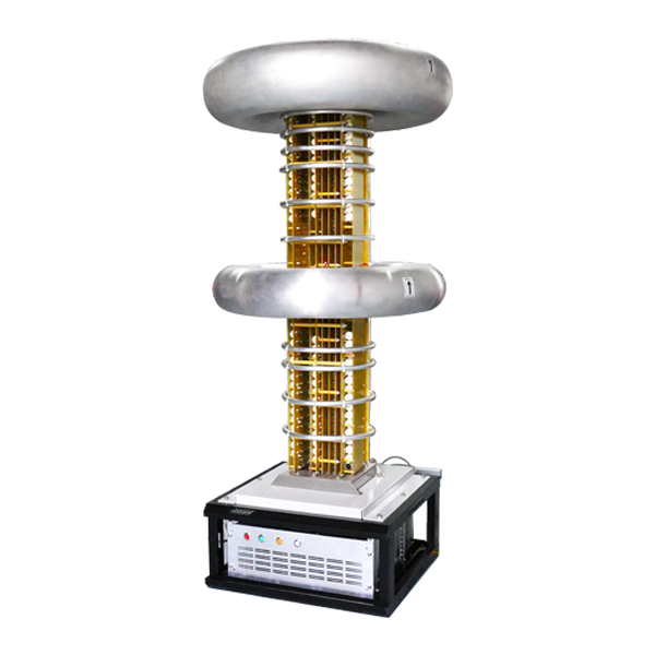
Phase-control technology adjusts three-phase AC voltage. DSPs or microcontrollers (e.g., TMS320F2812) serve as the core controller, collecting real-time electric field voltage and current signals. Upon detecting spark discharge (a sharp surge in secondary current), the system immediately blocks thyristor triggering pulses. After a delay, it recalculates the conduction angle to restore voltage to the critical discharge state, maximizing dust removal efficiency.
Pulse Modulation & Duty Cycle Optimization:
To counter adsorption force decay caused by external friction, an intelligent controller toggles the electrostatic output via reed relays within 10ms (frequency: 2–100Hz), resetting the dielectric layer’s charge distribution. Simultaneously, real-time voltage/current feedback adjusts the pulse duty cycle: reducing it when voltage exceeds the threshold by 5% and increasing it when current falls below the threshold by 5%, achieving dynamic adsorption equilibrium.
2. Material and Structural Synergy
Zoned Voltage Control:
For wafer warping-induced uneven gaps (up to 50μm at the center), multi-electrode arrays enable independent power supply. For example, a six-pole layout applies a baseline voltage (500V) to edge zones and elevates the center to 800V to compensate for adsorption loss.
Dielectric Material Innovation:
Johnson-Rahbek (JR) chucks use doped aluminum nitride ceramics to achieve adsorption forces comparable to traditional 3000V systems at just 800V, reducing arc risks. High-permittivity materials (e.g., barium titanate ceramics, εᵣ > 1000) replace alumina (εᵣ ≈ 10), increasing capacitance by 30% and boosting adsorption force by 30% at identical voltages.
3. Emerging Trends and Challenges
AI-Driven Control Loop:
Future systems will integrate machine learning to predict adsorption decay trends by analyzing parameters like wafer deformation and plasma interference, enabling dynamic voltage adjustments to form a sensing-decision-execution closed loop.
High-Frequency & Integrated Design:
Gallium nitride (GaN)-based switching power supplies (>500kHz) can triple power density and cut energy consumption by 60%, meeting compact device requirements.
Multi-Physics Field Coupling:
Coordinated control of electrostatic fields, thermal management (helium backpressure), and vibration suppression is critical. For instance, electrode layouts optimized through coupled electric-thermal field simulations can limit wafer temperature variations to ±0.5°C.
Conclusion
Intelligent control of electrostatic adsorption power supplies is evolving from single-parameter voltage adjustment to multi-parameter synergy, driven by sensing fusion, dynamic response, and material innovation. With advancements in wide-bandgap semiconductors and AI, these systems will further break precision barriers in manufacturing adsorption accuracy and energy efficiency.