Electromagnetic Shielding Design for High-Voltage Power Supplies in Electrostatic Chucks: Key Technologies and Applications
1 High-Voltage Power Supply Design: Core Challenges in Electrostatic Chuck Systems
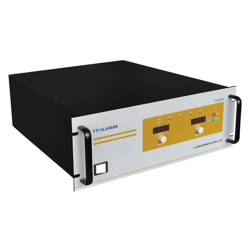
The electrostatic chuck (ESC), functioning as an invisible gripper in semiconductor manufacturing equipment, directly influences wafer processing precision and yield. In high-precision processes like plasma etching and ion implantation, ESCs utilize high-voltage power supplies to apply a strong electric field to electrodes, generating induced charges on the wafer's backside and achieving mechanical-free clamping through Coulomb forces. Based on operational principles, ESCs are mainly categorized into Coulomb types and Johnson-Rahbek (JR) types. Coulomb types require 3,000-4,000V high-voltage drive, while JR types need only 500-800V low voltage to generate stronger clamping forces due to the interface charge enhancement effect from doped semiconductor materials.
High-voltage power supply design faces three core challenges:
• Voltage Stability and Symmetry: Bipolar ESCs demand strictly symmetrical positive/negative electrode voltages (typically tolerance < ±1%). Voltage asymmetry causes micrometer-level displacement or even pattern distortion or wafer breakage. Traditional quadrupler voltage rectifier topologies suffer from complex current detection and poor voltage balancing. Advanced circuits employ commutation switches and PID closed-loop control with precision current-sensing resistors (e.g., Hall sensors or shunts) in diode series branches, achieving self-balancing functionality. When positive/negative current deviation exceeds thresholds, the system automatically adjusts PWM duty cycles to restore output symmetry.
• Plasma Environment Adaptability: Plasma in processing chambers induces self-bias effects on wafers, altering the ESC's actual potential distribution. Traditional solutions applying negative voltage compensation from the ESC bottom fail because DC voltage cannot effectively regulate plasma sheath potential. Advanced designs introduce 400kHz-2MHz low-frequency RF bias to dynamically compensate voltage drift while maintaining clamping stability.
• Fault Redundancy Mechanisms: Single-point failures in high-voltage supplies may cause instantaneous loss of clamping force, leading to wafer drops costing hundreds of thousands of dollars. Innovative architectures divide ESC electrodes into three independent power zones, each containing positive/negative electrode pairs connected to separate high-voltage supplies. When one zone fails (e.g., dielectric breakdown), other zones maintain >60% clamping force. Electrodes feature fan-shaped bases with interlocking convex-concave structures ensuring uniform insulation distribution.
Table: Comparison of Key Technologies for ESC High-Voltage Power Supplies
Technical Dimension Traditional Solution Advanced Solution Performance Improvement
Voltage Symmetry Quadrupler rectifier topology Commutation switches + PID control Asymmetry < ±0.5%
Bias Compensation DC negative voltage 400kHz-2MHz RF bias Sheath potential control accuracy >95%
Fault Redundancy Single power supply Triple-zone independent backup Clamping force >60% after single failure
Discharge Efficiency Passive leakage discharge Active commutation neutralization Residual charge clearance <50ms
2 Electromagnetic Shielding: Core Defense Against Interference
The strong electromagnetic fields from high-voltage power supplies coupled with high-frequency noise in plasma environments may trigger ESC malfunctions or control signal distortion. Effective electromagnetic shielding requires a multi-level protection system covering material selection, structural optimization, and grounding techniques.
2.1 Shielding Materials and Structural Optimization
• Conductive Continuity Design: Shielding effectiveness heavily depends on conductive continuity. Seams, cable openings, and vents become electromagnetic leakage sources. Electromagnetic sealing gaskets (e.g., conductive rubber or metal braids) fill gaps maintaining RF impedance below 10mΩ. Ventilation openings utilize honeycomb waveguide arrays based on cutoff waveguide principles (aperture < λ/5) to block electromagnetic waves above 30MHz while ensuring heat dissipation.
• Composite Shielding Structures: Single materials struggle against broadband interference. High-efficiency shields adopt layered composites: 0.5mm copper outer layer (reflection loss >80dB), μ-type ferrite absorbers (300kHz-1GHz band), and high-permeability alloy inner layer (e.g., permalloy). This design achieves >120dB shielding effectiveness (SE) from 10MHz-3GHz, significantly reducing power supply switching noise.
2.2 Grounding Techniques and Filtering Measures
• Grounding System Optimization: The key to electric shielding lies in grounding quality. ESC shields require grounding resistance <2mΩ (<0.5mΩ for critical applications) with grounding points near protected components. A star grounding topology separates high-voltage supply, control circuit, and sensor grounds to a central grounding point, avoiding ground loop coupling. Copper electrostatic shields between transformer windings with single-point grounding reduce high-frequency interference capacitance from 50pF to below 5pF.
• Multi-stage Filter Networks: Input power deploys π-type EMI filters with X-capacitors (line-line filtering), Y-capacitors (line-ground filtering), and common-mode chokes, achieving >60dB noise attenuation above 30MHz. DC outputs use LC-Γ composite filters reducing ripple to <0.1% at 10kV/1A. Signal lines incorporate feedthrough capacitors with ferrite beads suppressing high-frequency common-mode noise.
2.3 PCB Electromagnetic Compatibility Design
Circuit board layout critically impacts system stability:
• Power/Ground Plane Layering: Four-layer boards with solid ground planes provide low-impedance return paths
• Sensitive Circuit Isolation: PWM signal traces routed perpendicular to high-voltage lines with spacing >3× trace width
• Loop Area Minimization: Critical signals use differential pairs reducing loop area by >70%
• Decoupling Capacitor Arrays: Parallel 10μF tantalum and 0.1μF ceramic capacitors at power inputs suppress multi-band noise
Table: Electromagnetic Shielding Performance Evaluation for ESC Systems
Interference Type Shielding Measure Key Metric Optimization Effect
Power Conducted Emission π-type EMI filter + common-mode choke 30-100MHz insertion loss >60dB attenuation
Electric Field Radiation Copper/Permalloy composite shield 1GHz shielding effectiveness (SE) 120dB
Ground Line Interference Star grounding + low-resistance bonding Ground resistance <0.5mΩ
Signal Crosstalk Differential traces + ground plane isolation Crosstalk level ratio <-90dB
3 System Integration and Performance Optimization
High-voltage power supplies and electromagnetic shielding in ESCs require collaborative optimization:
3.1 Power-Shielding Co-Design
• Structural Layout Optimization: Mounting high-voltage modules directly beneath ESCs shortens high-voltage lines to <15cm, significantly reducing antenna effect radiation. Outputs use coaxial double-layer shielded cables with inner HV conductors, intermediate insulation, and grounded outer braiding, lowering spatial radiation by >40dB.
• Thermal-Electrical Co-Management: Integrating backside helium cooling channels maintains gas pressure at 20Torr (≈2,660Pa). Cooling gas acts as both thermal transfer medium and dielectric enhancer. Shield surfaces deposit 100nm aluminum nitride (AlN) coatings enhancing insulation strength (>15kV/mm breakdown field) and thermal conductivity (180W/mK).
3.2 Dynamic Bias and Intelligent Control
• Adaptive Voltage Compensation: Dynamic bias systems employ real-time current detection via precision shunt resistors (e.g., 5mΩ manganin) on transformer secondaries. When plasma-induced current deviation exceeds thresholds, RF bias compensation activates within 50μs.
• Coordinated Charge/Discharge Control: Innovative circuits solve residual charge issues. H-bridge commutation topology controls switch combinations (S1-S4) to reverse load current flow post-process, neutralizing residual charges within 50ms. Parallel discharge resistor networks ensure rapid force release.
4 Future Development Trends
As semiconductor manufacturing enters the sub-3nm era, ESC technologies face new challenges:
• Wide-Bandgap Semiconductors: SiC/GaN devices enable MHz switching frequencies, demanding shielding materials effective at higher frequencies. Novel nano-crystalline soft magnetic composites (Fe-Si-B-Nb-Cu systems) maintain initial permeability >20,000 at 3MHz with 90% lower eddy current losses.
• Smart Material Structures: Magnetorheological elastomer (MRE)-based adaptive shields dynamically adjust shielding bands by altering external magnetic fields.
• Multi-physics Co-simulation: Establishing electromagnetic-thermal-mechanical coupled models predicts shielding performance under extreme conditions. Simulations covering 10kHz-6GHz, 20-400°C, and 10⁻³-10³Pa provide design basis for complex environments.
Conclusion
The electromagnetic shielding design for high-voltage power supplies in electrostatic chucks represents a core technological challenge in semiconductor equipment manufacturing, directly impacting advanced process yields and reliability. Triple independent power redundancy enhances fault tolerance, composite shielding structures achieve broadband noise suppression, dynamic bias compensation solves plasma interference, and collaborative multi-physics optimization balances electrical-thermal-mechanical requirements—together forming a high-reliability solution for modern ESCs. Future breakthroughs in wide-bandgap semiconductors, smart materials, and multi-physics simulation will ensure exceptional ESC performance under higher-frequency, higher-temperature, and higher-vacuum extreme conditions, providing a solid foundation for the continued advancement of semiconductor manufacturing technology.