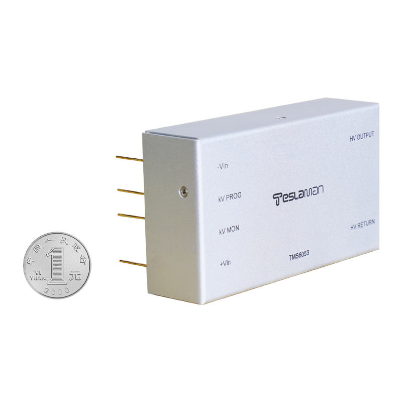
Monitoring Contact Resistance in High-Voltage Power Supplies for Electrostatic Chucks
In semiconductor manufacturing, electrostatic chucks (ESC) hold wafers via high-voltage electric fields, where the stability of the high-voltage power supply directly determines wafer flatness and temperature uniformity. Contact resistance between the power supply and chuck electrodes is a critical parameter—its minor fluctuations can cause adsorption failure or wafer damage. Thus, precise contact resistance monitoring is essential for process reliability.
Causes and Impact of Contact Resistance
Contact resistance comprises three components:
1. Constriction resistance: Caused by current concentration at contact points due to sudden cross-section changes;
2. Surface film resistance: Arises from oxide layers or contaminants on electrode surfaces;
3. Conductor resistance: Inherent resistance of electrode materials.
Surface film resistance is the primary variable. For example, rapid oxide formation (e.g., copper oxidizes in 2–3 minutes) or organic pollutant deposition increases resistance. In high-voltage fields, rising contact resistance triggers partial discharges or thermal runaway, leading to reduced adsorption force or electrode damage.
Monitoring Challenges and Solutions
1. High-Precision Measurement
Traditional two-wire methods fail at micro-ohm-level accuracy due to lead resistance interference. The mainstream solution is the four-wire (Kelvin) method:
• Principle: Separate current injection terminals (Drive+/Drive-) and voltage sensing terminals (Sense+/Sense-) eliminate lead and contact impedance effects.
• Implementation: A constant current (100mA–1A) is applied, while a high-impedance voltometer detects voltage drops across contacts. Resistance is calculated via Ohm’s law (R=U/I).
For high-voltage scenarios, voltage sensing lines must be placed directly near electrodes to avoid electromagnetic interference.
2. Dry Circuit Testing
Oxide layers on contacts may break down at 30–100mV, distorting measurements. Dry circuit technology limits open-circuit voltage ≤20mV and current ≤100mA to prevent oxide breakdown, revealing true film resistance. This is crucial for early-stage oxidation detection.
3. Dynamic Condition Adaptation
• Current Optimization: Low currents (e.g., 10mA) may fail to penetrate oxide films, yielding inflated readings. High currents (e.g., 100A) overcome contact issues but risk thermal effects. Multi-level current testing with trend analysis is recommended.
• Temperature Compensation: Contact resistance changes nonlinearly with temperature (e.g., copper oxide resistance spikes at high temperatures). Real-time temperature monitoring and compensation are essential.
System Implementation and Maintenance
1. Trend Analysis: Regular measurements under fixed positions and conditions track resistance trends. A >10% increase (based on process thresholds) signals electrode aging or contamination.
2. Anti-Interference Design:
• Use shielded twisted pairs to minimize high-voltage coupling;
• Six-wire methods further reduce errors in shunt structures, suitable for PCB-integrated electrodes.
3. Preventive Maintenance: Predict oxidation cycles based on resistance trends to schedule cleaning or replacement.
Conclusion
Contact resistance monitoring in ESC high-voltage power supplies is fundamental to semiconductor equipment reliability. Combining four-wire measurement, dry circuit technology, and dynamic compensation enables micro-ohm-level accuracy. As wafer processes advance below 3nm, real-time closed-loop control of contact resistance will integrate into power systems, becoming a key yield-enhancing technology.