High-Voltage Power Supply for Electrostatic Chucks: Critical Role of Surface Charge Monitoring
1. Working Principle of Electrostatic Chucks and Surface Charge Generation
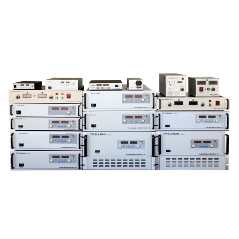
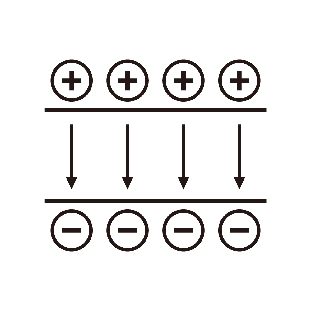
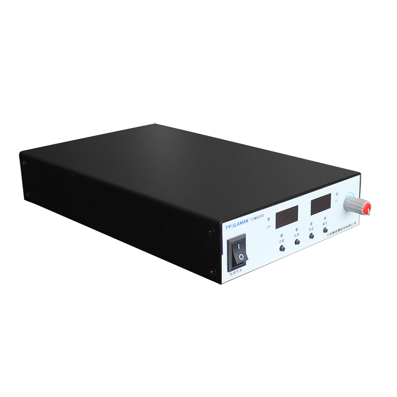
Electrostatic chucks (ESCs) utilize a high-voltage DC power supply (typically 500–4000 V) to generate an electrostatic field between electrodes and a dielectric layer (e.g., alumina ceramic), inducing opposite charges on the wafer backside. This creates Coulomb or Johnson-Rahbek forces for wafer clamping. The process is modeled as a parallel-plate capacitor: clamping force (F) is proportional to the square of voltage (V^2) and inversely proportional to the square of dielectric thickness (d^2), expressed as F \propto \frac{\varepsilon \cdot A \cdot V^2}{d^2} (\varepsilon: permittivity, A: effective clamping area).
During plasma processes (e.g., etching), residual charges accumulate on the wafer surface. If not dissipated, these charges cause wafer adhesion, handling misalignment (>3 mm triggers alarms), or microstructural damage.
2. Core Technologies for Surface Charge Monitoring
(1) Micro-Force Probe and Gas Backside Blow Method
A micro-force sensor (range: 0–100 mN, resolution: 0.1 mN) contacts the wafer surface to detect detachment from the ESC. Helium gas is injected (pressure: 20–2660 Pa) through the ESC backside. The critical gas pressures P_1 (upright) and P_2 (inverted) at detachment are recorded, and clamping force is calculated as:
\[ F = \frac{(P_1 P_2) \cdot S}{2} + G \]
(S: wafer area, G: wafer weight). This method offers <5% error and enables in-situ monitoring.
(2) Equivalent Capacitance and DC Filter Method
A DC filter (inductor L and grounded capacitor C_1) is connected in series to the ESC circuit. After processing, plasma is maintained to ground the ESC surface. Surface charge Q redistributes between the ESC’s bottom plate and C_1, and voltage U across C_1 is measured to derive charge density:
\[ Q = (C_{\text{esc}} + C_1) \cdot U \]
(C_{\text{esc}}: ESC equivalent capacitance). This achieves 0.5% accuracy for real-time quantification.
(3) Electrostatic Probe Scanning Method
A non-contact electrostatic probe (input impedance ≥1 TΩ) scans the wafer surface, combined with a 2D translation stage (positioning accuracy ±1.5 μm) to map surface potential. Inverse algorithms convert potential data into charge density profiles (±1 pC–20 μC resolution). The system operates in vacuum (<4×10⁻¹ Pa) to prevent air discharge interference.
3. Challenges and Future Trends
• Plasma Interference: DC voltage alone cannot modulate plasma sheath potential. Low-frequency RF bias (400 kHz–2 MHz) optimizes self-bias and stabilizes clamping.
• Resolution-Speed Trade-off: Traditional scanning is time-consuming. Novel techniques like Pulsed Electro-Acoustic (PEA) methods use nanosecond pulses and piezoelectric sensors (bandwidth 1 GHz) for dynamic charge mapping, applicable to high-voltage insulation materials.
• Material Innovation: High-permittivity dielectrics (e.g., doped AlN) enhance clamping at lower voltages; anti-corrosion coatings (PECVD-deposited) reduce residual charges.
Conclusion
Surface charge monitoring is pivotal for ESC reliability. Future advancements require multi-physics modeling (charge-electric-thermal coupling) and intelligent algorithms (e.g., leakage current analysis) to drive semiconductor manufacturing toward higher precision and stability.
