Research on Dielectric Interface Optimization of High-Voltage Power Supply for Electrostatic Chucks
The performance of electrostatic chucks (ESC), a core component in semiconductor manufacturing, relies on the synergistic interaction between high-voltage power supplies and dielectric interfaces. As the critical medium for electrostatic field transmission, the material properties, structural design, and electrothermal stability of dielectric interfaces directly affect wafer adsorption force distribution, positioning accuracy, and process repeatability. This article explores optimization pathways for dielectric interfaces under high-voltage power supply driving from three dimensions: material optimization, interface control technology, and system-level co-design.
I. Core Challenges of Dielectric Interfaces
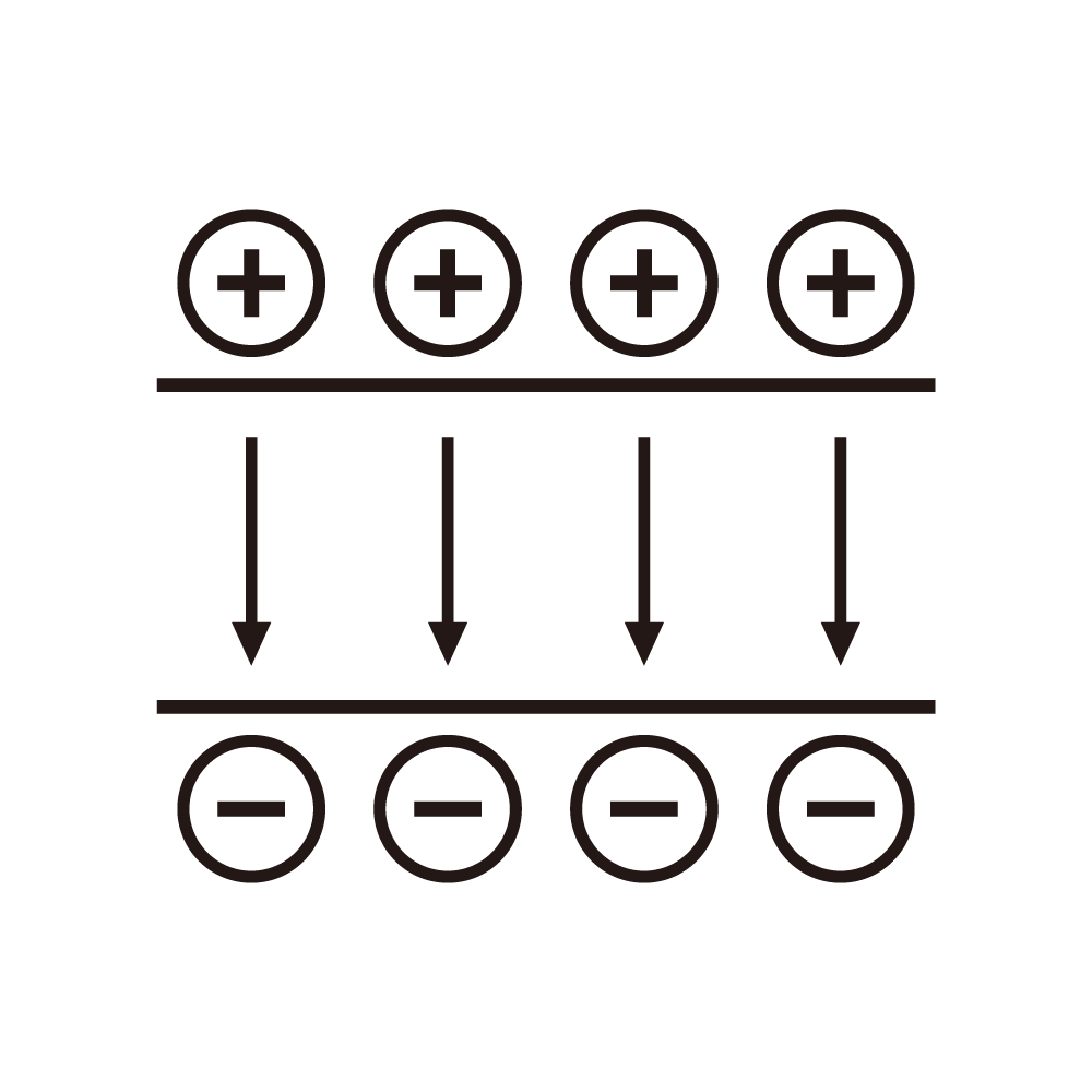
Electrostatic chucks generate Coulomb or Johnson-Rahbek forces by establishing an electrostatic field between the dielectric layer and wafer via high-voltage power. However, dielectric interfaces face multiple challenges:
1. Electrothermal Coupling Effects: Temperature drift in power output (e.g., 0.15% voltage drift per 10°C fluctuation) causes adsorption force instability, increasing wafer detachment risks.
2. Dielectric Performance Limits: Conventional alumina (Al₂O₃) layers have limited dielectric constants (ε≈9–10), restricting adsorption force enhancement. Volume resistivity variations at high temperatures also induce charge leakage.
3. Microscale Interface Defects: Microcracks or pores on dielectric surfaces trigger partial discharges under high electric fields, accelerating material aging and contaminating the process environment.
II. Dielectric Material Optimization Strategies
1. High-ε Material Applications
• AlN-Based Composites: Doping AlN with SiC adjusts volume resistivity while maintaining high thermal conductivity (≥180 W/m·K) and elevates ε>10, boosting adsorption force by 40% compared to traditional materials.
• Multilayer Composite Structures: Graded designs (e.g., Al₂O₃/AlN stacks) pair surface high-hardness layers for plasma resistance with high-ε underlayers to optimize electric field distribution, achieving adsorption force uniformity (<±0.8% fluctuation).
2. Functional Surface Coatings
• Anti-Plasma Coatings: Micron-thick diamond-like carbon (DLC) or boron nitride (BN) films deposited via PECVD reduce surface erosion and particle contamination.
• Micro-Nano Surface Structures: Etched micro-groove arrays (5–20 μm depth) increase effective adsorption area and enhance local adhesion through edge field intensification.
III. Interface Control Technology Breakthroughs
1. Temperature-Voltage Cooperative Compensation
• Second-Order Curvature Compensation: Combining PTAT (positive temperature coefficient) and CTAT (negative temperature coefficient) currents reduces power supply reference voltage drift from 35 ppm/°C to 3 ppm/°C, limiting output voltage drift to <0.005% within 25–100°C.
• Thermal Resistance Optimization: GaN-based switches with thermistor feedback networks suppress IGBT junction temperature fluctuations, maintaining >92% power efficiency and ΔT<15°C.
2. Dynamic Impedance Matching
• Gas dielectric constants in vacuum chambers vary with temperature (Δε/ΔT≈0.05%/°C), altering ESC equivalent capacitive loads. FPGA-controlled LC matching networks monitor load phase angles (±0.1° accuracy) and compensate resonant frequency within 200 μs, reducing adsorption force fluctuation from ±5% to ±0.8%.
3. Edge Field Optimization Algorithms
• Finite element simulations (e.g., COMSOL) model electric fields at dielectric-wafer interfaces to optimize edge electrode field distribution. Arced electrodes enhance edge adsorption force by 25%, preventing wafer edge warpage.
IV. System-Level Co-Optimization Pathways
Dielectric interface performance requires integrated power supply architecture upgrades:
• Multilevel Topology: Half-bridge series circuits replace mechanical relays, enabling polarity switching in <300 ms (vs. >1 s traditionally) and supporting arbitrary waveforms for complex processes.
• Digital Twin Predictive Models: Multi-physics simulations (electrical-thermal-mechanical) predict interface behavior under varying process parameters (e.g., RF power, pressure), enabling dynamic high-voltage output adjustments.
Conclusion
Optimizing dielectric interfaces for ESC high-voltage power supplies represents interdisciplinary innovation spanning materials science, power electronics, and control algorithms. Integrating high-ε composites, temperature-voltage compensation, and dynamic impedance matching can establish near temperature-invariant adsorption systems. Future advancements in wide-bandgap semiconductor devices and AI-driven real-time control will further extend the boundaries of nanoscale process precision, providing semiconductor manufacturing with a more stable invisible hand.
