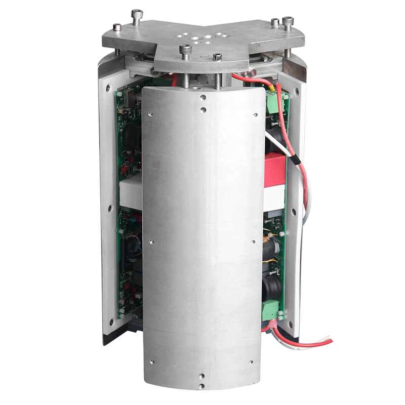
Methods for Suppressing Radiation Noise in High-Voltage Power Supplies of Lithography Machines
Lithography machines, as core equipment in semiconductor manufacturing, face challenges where radiation noise from high-voltage power supplies can interfere with precision optical systems and control circuits, leading to wafer exposure defects. This noise primarily originates from high-frequency switching (kHz~MHz range) in power supplies, PCB layout flaws, and common-mode current loops. Key suppression techniques are detailed below from three perspectives: noise source control, circuit optimization, and system protection.
1. Noise Source Suppression
• Switching Frequency Optimization:
Adjust the voltage slew rate (dv/dt) of power switching devices to prevent high-frequency harmonics. Spread Spectrum Frequency Modulation disperses fixed switching frequencies into a narrow band, reducing peak noise at specific frequencies.
• Low-Noise Component Selection:
Use ultra-fast recovery diodes (trr ≤25ns) to minimize transient reverse currents and soft-switching topologies (e.g., LLC resonance) for zero-voltage switching (ZVS), eliminating MOSFET switching noise.
2. PCB and Grounding Design
• Multilayer Stackup:
Adopt ≥4-layer designs with adjacent power and ground planes (spacing ≤0.2mm) to form distributed capacitance and reduce impedance. Split power planes into isolated analog/digital zones to avoid coupled noise.
• Star-Point Grounding:
Connect digital and analog grounds via beads or 0Ω resistors at a single point. High-current paths (e.g., stepper motors) use dedicated grounds to prevent common-mode contamination. Use ≥3mm-wide traces with gridded copper pours for low impedance.
• Critical Path Optimization:
Shorten high-voltage traces, avoid sharp bends, and place ground via arrays (spacing ≤λ/10) beneath switches/transformers to absorb radiation.
3. Filtering and Shielding
• Multi-Stage Filtering:
• Input Stage: π-filters (X-cap + common-mode choke) suppress differential-mode noise.
• Output Stage: LC filters (low-ESR ceramic capacitors + ferrite beads) attenuate ripple, with LDOs added for secondary regulation.
• Common-Mode Suppression:
Install Ni-Zn ferrite cores (impedance ≥1kΩ@100MHz) on power cables, winding 2~3 turns to increase common-mode impedance.
• Electromagnetic Shielding:
Encase power modules in mu-metal shields with conductive gaskets at seams. Use ceramic-based thermal pads between MOSFETs and heatsinks to avoid antenna effects from single-point grounding.
4. System-Level Protection
• Dual-Power Redundancy:
Deploy static transfer switches (STS) with ≤20ms switching to ensure uninterrupted UPS backup during grid sags, preventing abrupt noise.
• Structural Leakage Control:
Seal cable ports with copper braids and use honeycomb waveguide vents (cutoff frequency >1GHz) to block radiation leaks.
Validation and Testing
Radiation tests require anechoic chambers with background noise >6dB below limits. Critical bands (30MHz~1GHz) are scanned using near-field probes to locate noise sources. Post-optimization targets include:
• Conducted noise (CISPR 25): Peak ≤60dBμV (150kHz~30MHz);
• Radiated noise (CISPR 32): Average ≤40dBμV/m (30MHz~1GHz).
Summary: Effective noise suppression in lithography power supplies demands co-design of circuits, PCB processes, and system shielding. Core strategies involve minimizing common-mode loop areas, optimizing high-frequency impedance, and blocking noise propagation through multi-stage filtering. Implementation reduces radiation noise by 20~40dB, ensuring sub-nanometer exposure accuracy.
