Breakthrough in Nanometer-Level Ripple Suppression Technology for High-Voltage Power Supplies in Electron Microscopy
The stability of high-voltage power supplies directly impacts the imaging precision of transmission electron microscopes (TEM). In nanoscale observations, output voltage ripple must be controlled at millivolt or even microvolt levels; otherwise, electron beam energy fluctuations, blurred sample images, and reduced resolution may occur. Traditional power supply ripple primarily originates from high-frequency switching noise, low-frequency input fluctuations, and parasitic parameter interference. High-voltage power supplies for TEM (typically 80–300 kV) require multidisciplinary technologies to achieve extreme ripple suppression.
1. Technical Challenges in Ripple Suppression
• High-Frequency Ripple: MOSFET switching in power supplies generates hundreds of kilohertz of noise, whose harmonics easily couple to the output through parasitic capacitance.
• Low-Frequency Ripple: Grid input fluctuations leave residual power-frequency ripple (50–100 Hz) after rectification and filtering, necessitating high-gain feedback loops for suppression.
• Common-Mode Noise: Parasitic capacitance between transformer windings and heat sinks creates common-mode pathways, leading to current loop imbalances.
For example, in a 10 kV high-voltage power supply, ripple exceeding 0.001% directly results in loss of detail in sub-nanoscale imaging.
2. Advanced Suppression Architectures and Practical Solutions
Multi-Stage Filtering and Topology Optimization
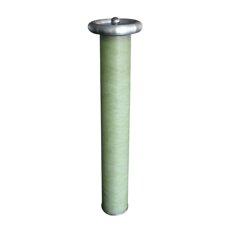
A Royer inverter architecture combined with a voltage doubler rectifier circuit stabilizes the switching frequency at 67–76 kHz, reducing high-frequency harmonic generation. Through a 12-stage voltage doubler rectifier and a low-equivalent-series-resistance (ESR) ceramic capacitor array, ripple peak-to-peak values ≤2 V@10 kV are achieved—a 50% reduction compared to traditional solutions.
Dynamic Feedback and Ripple Compensation
• Digital Feedback Control: Microcontrollers sample the output voltage in real time, dynamically adjusting PWM duty cycles via PID algorithms to suppress low-frequency fluctuations. Experiments show that with enhanced closed-loop gain, low-frequency ripple attenuation reaches 40 dB.
• Active Compensation Circuit: Injects an inverted ripple signal into the output to cancel native noise. This technique achieves >90% suppression efficiency for ripple below 1 kHz and performs reliably across wide temperature ranges.
Hardware-Level Elimination of Common-Mode Noise
A star grounding topology and multi-layer shielding in PCB layout reduce parasitic capacitance below 0.5 pF. Simultaneously, common-mode chokes and Y-capacitors attenuate common-mode ripple by 60 dB.
3. Technology Trends and Application Prospects
• Wide-Bandgap Semiconductors: Gallium nitride (GaN) devices support MHz-level switching frequencies, reducing filter component size and improving efficiency.
• Hybrid Power Architecture: A front-stage switching supply paired with a rear-stage linear regulator (LDO) balances efficiency with nanometer-level ripple requirements, making it suitable for life science instruments like cryo-electron microscopes.
Currently, domestic high-voltage power supplies have achieved a breakthrough ripple coefficient of 0.0003%, advancing materials science and semiconductor inspection into the sub-angstrom (<0.1 nm) resolution era. Future developments leveraging AI-based adaptive ripple compensation algorithms will further enhance stability under complex loads.
In summary, nanometer-level ripple suppression in high-voltage power supplies demands innovations in circuit topology, digital control algorithms, and precision manufacturing. As domestically developed advanced TEMs rise, these technologies will break import dependencies and provide foundational support for cutting-edge research.