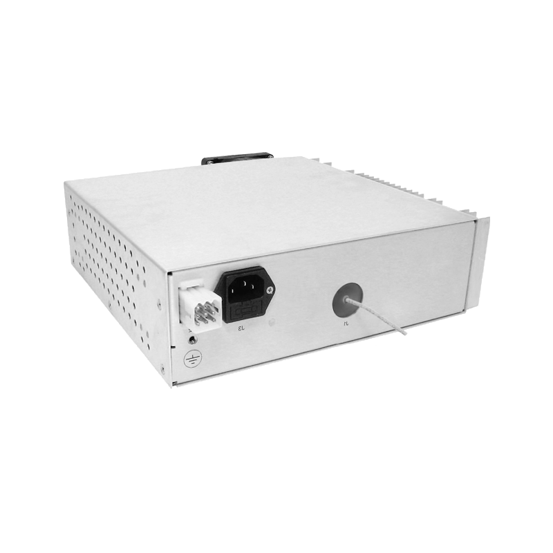
Research on Efficiency Improvement of High-Voltage Power Supplies for Lithography Exposure Machines
Lithography exposure machines are core equipment in semiconductor manufacturing and precision photolithography, where imaging quality directly depends on the stability and efficiency of high-voltage power supplies. Traditional high-voltage power supplies face issues such as high energy consumption, significant thermal losses, and bulky size, which limit improvements in exposure precision and device miniaturization. This article explores efficiency enhancement paths for high-voltage power supplies in exposure machines from four aspects: device selection, topology optimization, thermal management, and control strategies.
1. Application of Novel Power Devices
Wide-bandgap semiconductor devices like silicon carbide (SiC) and gallium nitride (GaN) are key to breaking efficiency barriers in high-voltage power supplies. Compared to traditional silicon-based devices, SiC-MOSFETs and SiC-SBDs (Schottky Barrier Diodes) offer higher switching frequencies (exceeding 50 kHz), lower conduction losses (reduced by 85%), and high-temperature tolerance (operating temperature >200°C). In exposure machine high-voltage modules, replacing conventional silicon rectifiers with SiC-SBDs significantly reduces reverse recovery losses and addresses voltage-sharing issues under high-frequency conditions. Experiments show that all-SiC-based power supplies achieve 15%-20% higher efficiency and 50% smaller volume.
2. Optimization of Topology and Resonant Technology
Exposure machine high-voltage power supplies often adopt series-parallel resonant (LCC) charging topologies, which reduce switching losses by achieving zero-voltage switching (ZVS) through resonant parameter (inductance, capacitance) tuning. Examples include:
• Adaptive Off-Time Control Algorithms: Maintain current-limited continuous mode in flyback topologies to avoid inrush currents, increasing efficiency to over 75% (compared to 50%-60% in traditional solutions).
• Modular Multi-Stage Design: Decompose high-voltage generation circuits into series-connected sub-modules with digitalized voltage balancing, reducing single-module boosting pressure while expanding power capacity (up to MW level).
3. Thermal Management and EMC Design
High temperature is a primary cause of efficiency degradation. Optimization measures include:
• Integrated Thermal Management: Combining heat collectors, radiators, and enclosures for conduction cooling (operating temperature ≤45°C).
• High-Frequency Transformer Encapsulation: Using vacuum epoxy potting and segmented winding to minimize leakage inductance and distributed capacitance, suppressing eddy current losses.
• Electromagnetic Shielding: Copper/steel Faraday cages combined with cable shielding layers reduce RF interference to control circuits.
4. Intelligent Control Strategies
Digital control is essential for dynamic efficiency optimization:
• Load-Adaptive Regulation: Real-time PWM feedback adjusts duty cycles, switching to eco-mode under light loads (standby power <1 W).
• Multi-Stage Voltage Stabilization: A first-stage DC/DC module (efficiency >95%) and a second-stage high-frequency inverter with transformer boosting achieve a combined ripple factor <0.1%.
5. Future Trends
High-voltage power supplies are evolving toward higher frequencies, solid-state designs, and intelligence. Combining SiC devices with AI-driven control algorithms will further break efficiency barriers (target >90%). Additionally, digital twin-based virtual testing can shorten R&D cycles by 20%-50%, accelerating applications in cutting-edge fields like extreme ultraviolet (EUV) exposure machines.