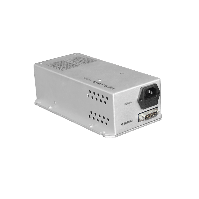
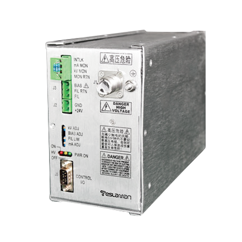
Research on Wafer Adsorption Force Technology of E-Chuck High Voltage Power Supply
1. Electrostatic Adsorption Principle and Technical Requirements
In semiconductor manufacturing, a critical challenge lies in achieving stable fixation and damage-free transfer of wafers. Traditional mechanical clamping risks surface scratches or particulate contamination, whereas electrostatic adsorption technology (E-Chuck) based on high-voltage power supplies enables non-contact fixation through electric field forces. The principle involves applying kilovolt-level DC or pulsed voltage to electrodes via a high-voltage power supply, creating an electrostatic field between the wafer and the adsorption surface to generate Coulomb forces. Studies show that adsorption force intensity is proportional to the square of the electric field strength, making voltage stability and dynamic response capabilities of the power supply decisive factors.
2. Technical Challenges and Innovations
1. Micro-Discharge Suppression: High-voltage operation in kilovolt ranges risks air ionization and micro-discharge, leading to adsorption force fluctuations or wafer damage. Optimized electrode structures (e.g., multi-layer shielding and gradient field distribution) combined with high-frequency modulation technology elevate discharge thresholds above 15kV/mm, reducing energy loss significantly.
2. Dynamic Response Control: Millisecond-level adsorption/release switching during wafer transfer demands precision. Digitally controlled power modules with PID closed-loop algorithms achieve voltage regulation accuracy within ±0.05% and response times under 50μs, meeting high-speed production requirements.
3. Environmental Adaptability: Semiconductor workshops face electromagnetic interference and temperature fluctuations. Enhanced packaging (ceramic substrates with metal casings) and multi-stage filtering circuits limit voltage drift to <0.1% across -40°C~85°C, with electromagnetic immunity reaching 100V/m.
3. Technological Evolution and Industry Impact
1. Process Compatibility: For 300mm wafers, zone-specific voltage adjustment technology uses arrayed electrodes and independent power modules to achieve localized adsorption force control (0.1N/cm²~5N/cm²), compatible with sub-5nm warped wafers.
2. Energy Efficiency: Resonant power topologies boost conversion efficiency to 92%, cutting energy consumption by 40% compared to linear supplies. Dynamic voltage scaling further reduces energy use by 35% in standby modes.
3. Intelligent Systems: Integrated IEPE sensors and edge computing modules monitor pressure distribution in real-time, auto-adjusting voltage parameters. This innovation lowers wafer breakage rates from 0.01% to 0.0015%, improving yield by 1.2%.
4. Future Development Trends
1. Hybrid Field Technology: Electromagnetic-electrostatic hybrid adsorption could address deformation in ultra-thin wafers (<50μm) via Lorentz force compensation, potentially enhancing adsorption uniformity to 98%.
2. Material Advancements: Wide-bandgap semiconductors (e.g., GaN-on-Diamond) may extend operational voltages to 30kV while reducing module size by 60%.
3. Digital Twin Integration: Machine learning-based predictive models enable virtual parameter optimization, potentially slashing equipment commissioning time by over 70%.