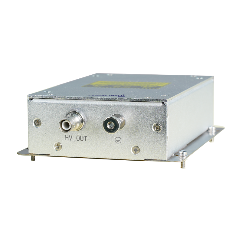
Radiation-Resistant Shielding Structure Design and Application for High-Voltage Power Supplies in Lithography Machines
In the manufacturing of semiconductor nanoscale processes, lithography machines are core equipment, and their operational precision directly determines chip yield. As a key power unit of lithography machines, the high-voltage power supply (HVPS) is responsible for providing stable high-voltage output to core components such as laser systems and electrostatic chucks. However, under high-frequency and high-voltage operating conditions, it tends to generate electromagnetic radiation. Meanwhile, the external radiation environment may also interfere with the stability of the power supply’s output. Therefore, the radiation-resistant shielding structure has become a crucial link in ensuring the overall performance of lithography machines.
The radiation interference faced by the HVPS of lithography machines is bidirectional. On one hand, the high-voltage rectifier modules and high-frequency inverter circuits inside the power supply produce wide-band electromagnetic radiation during operation. Among this radiation, high-frequency waves can easily penetrate conventional enclosures, interfering with the laser positioning system and precision displacement platform of the lithography machine, and causing nanoscale deviations in lithographic patterns. On the other hand, there are multiple high-power devices (such as ion implanters and etchers) in semiconductor workshops. The external radiation generated by these devices may couple into the HVPS, increasing the ripple of the output voltage and affecting the operational stability of load components.
The design of the radiation-resistant shielding structure must focus on the dual goals of suppressing radiation leakage and resisting external interference, with the core lying in the synergy between material selection and structural optimization. For material selection, a single metal cannot meet wide-band radiation protection needs, so a high magnetic permeability-high electrical conductivity composite structure is often adopted. The inner layer uses Permalloy, which leverages its excellent low-frequency magnetic field shielding capability to attenuate low-frequency radiation inside the power supply. The outer layer uses oxygen-free copper plates, which reflect high-frequency electromagnetic radiation through their high electrical conductivity while reducing the eddy current loss of the shield itself. To avoid signal reflection at the material interface, the two layers must be tightly bonded via vacuum diffusion welding to minimize radiation leakage channels caused by interface gaps.
In structural design, the shield enclosure must address the key issue of gap leakage. Splicing joints of the HVPS enclosure (such as the connecting flange between the cover plate and the main body) are prone to forming radiation leakage windows due to assembly gaps. Thus, conductive gaskets are used for sealing—finger-shaped gaskets made of beryllium copper are selected. Their elastic structure ensures the flange surface maintains tight contact under long-term vibration, and the high conductivity of beryllium copper controls radiation leakage at gaps to below 10dB. In addition, dedicated shielding components must be designed for the power supply’s cable interfaces and heat dissipation holes: cable interfaces use filter connectors to filter out high-frequency interference signals via feedthrough capacitors; heat dissipation holes adopt a honeycomb structure, with the size of honeycomb holes designed to be less than 1/20 of the wavelength of the protected frequency band, ensuring both heat dissipation efficiency and radiation penetration prevention.
To verify the effectiveness of the shielding structure, a multi-dimensional testing system is required. In an EMI anechoic chamber, a broadband antenna is used to detect the radiation field strength outside the shield, ensuring the radiation value meets electromagnetic compatibility standards for semiconductor equipment in the 30MHz-1GHz band. Meanwhile, an external strong radiation environment is simulated to test the shielding structure’s protective effect on the internal power supply output—it is required that when the external radiation intensity increases by 10 times, the ripple change rate of the power supply’s output voltage does not exceed 0.1%. Additionally, long-term reliability tests need to simulate the 100,000-hour operation cycle of the lithography machine, and verify the bonding strength of shielding materials and the elastic attenuation of conductive gaskets through temperature cycling, vibration testing, and other methods to ensure no significant degradation of shielding performance.
The design of the radiation-resistant shielding structure for the HVPS of lithography machines essentially solves the core contradiction of radiation interference-precision loss through the integration of materials science and structural engineering. As semiconductor processes advance to the 3nm node and below, the sensitivity of lithographic precision to radiation interference further increases. The shielding structure will develop toward ultra-thinness and integration. In the future, the shielding layer may be integrated with the heat dissipation structure of the power supply enclosure, ensuring radiation protection performance while reducing the overall volume and weight of the equipment, and providing support for the precision development of lithography machines.