Multi-Physics Field Collaborative Control of High-Voltage Power Supply for Electrostatic Chuck
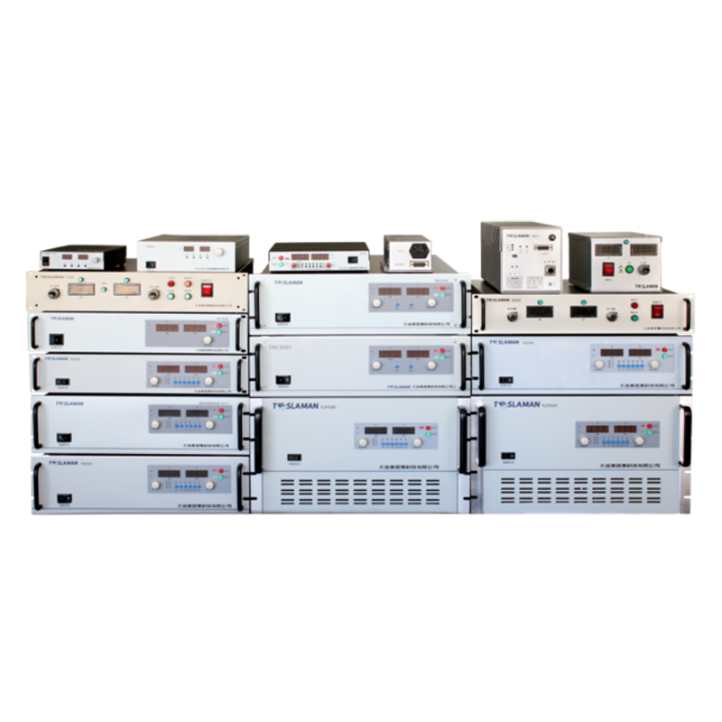
In the wafer processing of advanced semiconductor processes (such as 3nm and below), the electrostatic chuck (ESC) is a core component for achieving high-precision positioning and stable clamping of wafers, and its performance directly depends on the output quality and control accuracy of the high-voltage power supply (HVPS). However, there exists a strong coupling effect among the electric field, temperature field, and stress field during the operation of the ESC: the electric field provides the electrostatic force required for clamping, the temperature field changes dynamically due to power supply losses and process heat generation, and the stress field originates from uneven clamping force and thermal deformation. The mutual interference among the three fields easily leads to reduced clamping accuracy, wafer damage, or process failure. Traditional independent control schemes for single physical fields are unable to address the complex challenges brought by multi-field coupling. Therefore, multi-physics field collaborative control of high-voltage power supply for electrostatic chucks has become a key technical direction to break through the precision bottleneck in advanced semiconductor manufacturing.
The multi-physics field coupling of the electrostatic chuck high-voltage power supply system exhibits significant dynamic correlation. From the perspective of the electric field, the stability of the HVPS output voltage determines the magnitude of the electrostatic force. If the voltage fluctuation exceeds ±1%, the clamping force deviation will exceed 5%, directly affecting wafer flatness. In terms of the temperature field, the heat generated by the HVPS power module (with a typical loss of 50-100W) and the local high temperature (up to 150°C) during wafer etching will change the temperature of the ESC dielectric layer. The temperature coefficient of the dielectric constant is approximately -0.002/°C, and each 1°C fluctuation in temperature will cause a 0.2% deviation in electric field strength, forming a temperature-electric field negative feedback. Regarding the stress field, uneven electrostatic force can cause the wafer to deform by a maximum of 0.5μm. This deformation further changes the distance between electrodes, which in turn interferes with the electric field distribution. At the same time, when the stress exceeds 10MPa, it may cause lattice damage to the wafer, reducing device yield.
Multi-physics field collaborative control requires the construction of a closed-loop system of perception-decision-execution. The perception layer adopts a high-precision sensor array to collect parameters at a frequency not lower than 1kHz: an electric field sensor (with an accuracy of ±0.1kV/m) monitors the electric field distribution of the electrodes, an infrared temperature measurement module (with a resolution of ±0.1°C) captures the temperature field of the dielectric layer, and a piezoelectric stress sensor (with a range of 0-50MPa) obtains the wafer stress state. The decision-making layer introduces a multi-variable model predictive control (MPC) algorithm, which establishes a correlation equation among the three fields based on the coupled dynamic model. Under the constraints of voltage ≤ 3kV, temperature ≤ 120°C, and stress ≤ 8MPa, it dynamically optimizes the HVPS output parameters and auxiliary adjustment instructions. Compared with traditional PID control, the control deviation can be reduced by more than 60%. The execution layer realizes cross-module collaboration: the HVPS adjusts the output voltage in real time through pulse width modulation (PWM), and at the same time links with the temperature control module (such as a micro water-cooling channel) and the stress compensation mechanism. The response delay of the three is controlled within 10ms to ensure the synchronous optimization of multi-field parameters.
This technology can significantly improve the process stability of advanced manufacturing processes. In 3nm wafer etching, it can control the clamping force fluctuation within ±2%, reduce the temperature fluctuation to ±0.3°C, and lower the wafer deformation to less than 0.1μm, which directly reduces the wafer damage rate by 30% and increases the process yield by 5%-8%. At the same time, it can adapt to the switching needs of wafers of different sizes (such as 12-inch and 18-inch) without frequent adjustment of control parameters, reducing equipment debugging time by approximately 40% and providing core support for the high efficiency and high precision of semiconductor manufacturing.
In conclusion, the multi-physics field collaborative control of the high-voltage power supply for electrostatic chucks solves the problem of multi-field coupling and realizes the global optimization of the electric field-temperature field-stress field, making it an indispensable key technology in advanced semiconductor manufacturing. In the future, with the integration of AI algorithms and high-precision sensing technology, this control scheme will further improve the dynamic response speed and adaptability, providing more reliable technical support for wafer processing of higher processes (such as 2nm and below).
