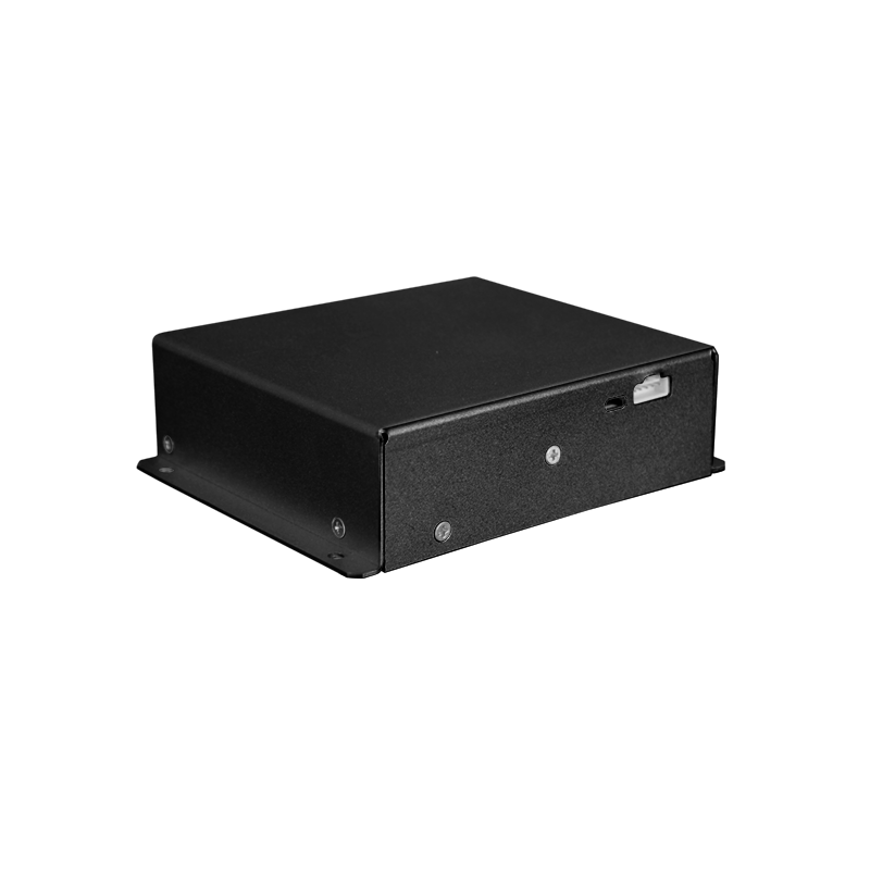
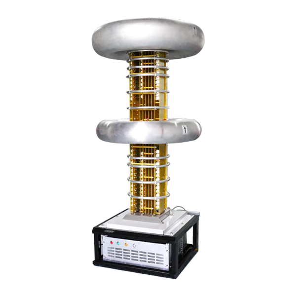
Noise Source Tracing and Control of High-Voltage Power Supply for Lithography Exposure Machines
In the precision lithography manufacturing system, the lithography exposure machine is a core piece of equipment, and its imaging accuracy directly determines the final yield of chip manufacturing processes. As the energy core of the exposure machine's light source module, the high-voltage power supply (HVPS) has output noise that directly affects the stability of the light beam through the light source drive link. This, in turn, leads to key issues such as linewidth uniformity deviations and overlay accuracy degradation. Therefore, accurately tracing the noise of the high-voltage power supply and formulating targeted control strategies are core links to ensure the precise operation of the exposure machine.
The noise source tracing of the high-voltage power supply for exposure machines should be carried out from two dimensions: internal source and external coupling. From the perspective of internal structure, noise mainly originates from the nonlinear characteristics of the power conversion link. Firstly, in the phase-shifted full-bridge or LLC resonant topologies commonly used in high-voltage power supplies, the high-frequency on-off of power switches (such as IGBTs and SiC MOSFETs) generates voltage spikes. Especially when the switching frequency resonates with the circuit's parasitic parameters (transformer leakage inductance, bus capacitor ESR), the spike amplitude can reach 15%-20% of the rated output, forming pulse-like noise. Secondly, in the high-voltage rectification and filtering unit, the reverse recovery current of fast recovery diodes causes current mutations, generating ripple noise across the loop impedance. This noise superimposes exponentially as the output voltage increases. From the perspective of external coupling paths, noise propagation is divided into two categories: one is conductive coupling, where voltage fluctuations on the power grid intrude through the input power line and interfere with the output after superimposing with internal power supply noise; the other is radiative coupling, where the high-voltage output leads, due to their high voltage level (usually kV level), easily form an electromagnetic radiation field, which interferes with the photoelectric detection circuits and servo control circuits inside the exposure machine, resulting in a decrease in the signal-to-noise ratio of detection signals. In addition, the dynamic changes of the light source load during the exposure process (such as the sudden change of the lamp current from the standby state to the working state) will cause the instantaneous imbalance of the output impedance of the high-voltage power supply, further intensifying noise fluctuations.
To address the above noise sources, a three-level control system of source suppression path blocking load adaptation should be established. At the source suppression level, soft-switching technologies (zero-voltage switching ZVS, zero-current switching ZCS) are used to optimize the power conversion process, reducing the overlap area of the switch's voltage and current to the microsecond level and lowering the amplitude of switching noise. Meanwhile, an RLC snubber circuit is designed in the power loop to offset voltage spikes and current ripples by matching the resonant frequency of parasitic parameters. At the path blocking level, an EMI filter integrating differential-mode inductors, common-mode inductors, and X/Y capacitors is configured on the input side to suppress grid noise conduction; the high-voltage output leads adopt a double-layer shielding structure (inner shielding layer grounded, outer shielding layer floating) to reduce the intensity of radiative coupling; the PCB layout adopts a partitioned design of power area control area sensitive area, and the sensitive circuits use single-point grounding to avoid ground loop noise interference. At the load adaptation level, an adaptive PID control algorithm is introduced. By real-time sampling the current changes of the light source load, the driving signal of the power switch is dynamically adjusted to maintain the matching between the output impedance of the high-voltage power supply and the load impedance, controlling the noise fluctuation caused by dynamic loads within 5mV.
The noise control of the high-voltage power supply for exposure machines is essentially a systematic project. It is necessary to clarify the dominant factors of noise through accurate source tracing, and then realize effective noise suppression by combining topology optimization, electromagnetic compatibility design, and control algorithm collaboration. This process not only improves the imaging accuracy of the exposure machine but also provides a reusable noise control paradigm for the application of high-voltage power supplies in the field of precision manufacturing, contributing to the performance breakthrough of high-end equipment.