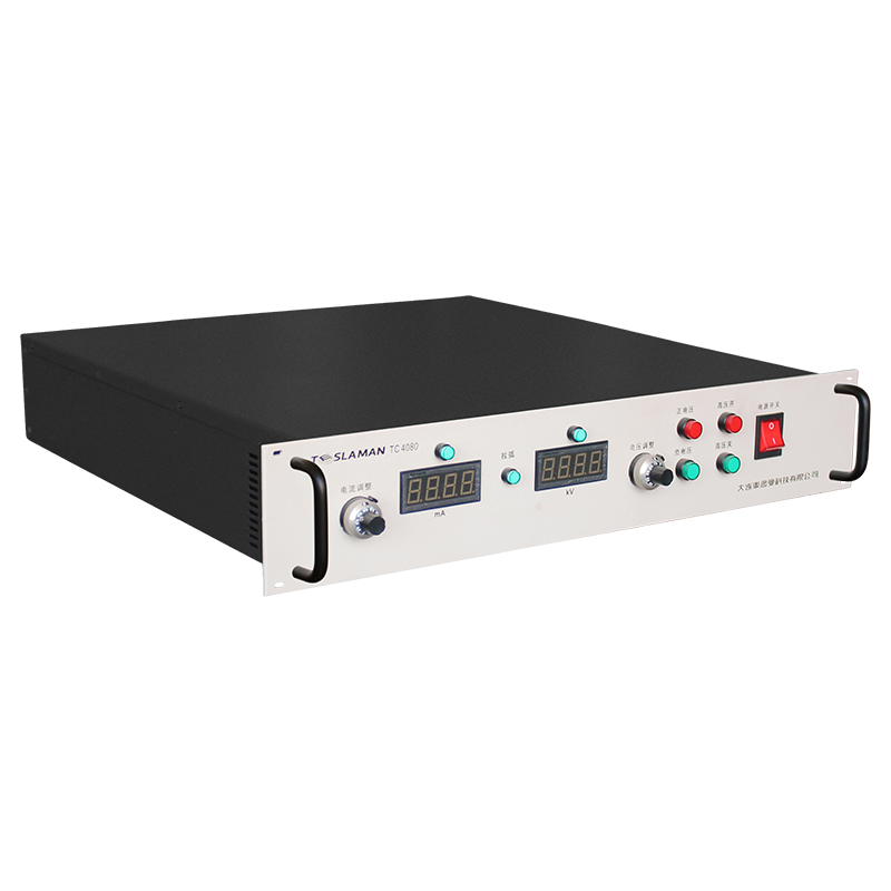
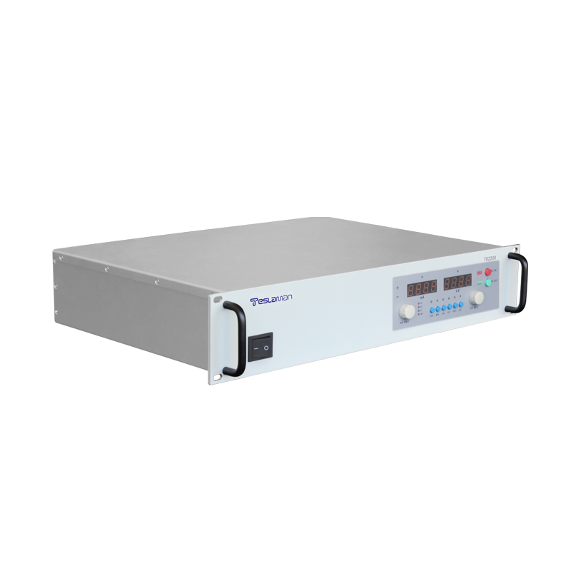
Application of High-Voltage Power Supply in Atomic-Level Surface Charge Neutralization for Electron Microscopes
As a core tool for characterizing the microcosmic world, electron microscopes (EM) have advanced from micron-level resolution to the era of atomic-level observation. However, the accumulation and imbalance of surface charges on samples have become a key bottleneck restricting the accuracy of high-resolution imaging. Against this backdrop, high-voltage power supplies (HVPS), by precisely regulating energy and beam current to achieve atomic-level surface charge neutralization, have emerged as a core supporting technology for electron microscopes to exert their ultimate performance. Their application value has penetrated into cutting-edge research fields such as semiconductors, two-dimensional (2D) materials, and biological macromolecules.
From the perspective of technical principles, the generation of surface charges on samples during EM observation stems from the interaction between the incident electron beam and the sample. The imbalance between the injection of incident electrons and the emission of secondary electrons leads to the accumulation of positive or negative charges on the sample surface (especially for insulating or low-conductivity samples), causing charge contrast interference and even distorting atomic-level topographic signals. The core function of the HVPS is to output a stable high-energy beam (electron beam or ion beam) as a neutralization source to precisely match the charge density on the sample surface. On one hand, the HVPS must achieve an energy accuracy of within ±0.1%, ensuring that the energy of the neutralization beam exactly offsets the excess charges on the surface—avoiding damage to the sample’s atomic structure due to excessively high energy or incomplete neutralization due to excessively low energy. On the other hand, its beam current ripple must be suppressed to the nanoampere (nA) level, ensuring the spatial uniformity of the neutralization beam and thereby realizing the balance of charge distribution at the atomic scale.
In practical applications, the atomic-level charge neutralization capability of HVPS has become a core technology for breaking through observation bottlenecks in key fields. In the semiconductor industry, the interface charges between insulating and conductive layers in FinFET structures of chips with 7nm and smaller processes tend to blur EM images. By dynamically regulating the neutralization beam current, HVPS can real-time offset charge accumulation at the interface, clearly revealing atomic-level defects (such as vacancies and dislocations) and providing a direct observation basis for improving chip yield. In the research of 2D materials, the surface charges of single-layer materials (e.g., MoS₂ and graphene) are highly susceptible to environmental interference. The low-energy electron beam (10-50eV) output by HVPS can achieve charge neutralization without damaging the lattice structure, helping researchers observe atomic-level interlayer stacking patterns and defect evolution. In the field of cryo-EM for biological research, charges on the surface of biological macromolecules (e.g., protein complexes) can cause electron beam deflection. The coordinated control of HVPS and low-temperature systems can minimize charge interference, significantly improving the resolution of 3D reconstruction and enabling the analysis of the atomic-level structure of biomolecules.
Currently, this technology still faces three major challenges: first, the dynamic charge response issue—changes in sample morphology (e.g., structural evolution during in-situ reactions) lead to real-time fluctuations in charge distribution, requiring HVPS to have a response speed at the microsecond level; second, the adaptability to multi-beam EMs—when multiple beams are used for parallel imaging, multiple sets of HVPS must achieve nanoscale synchronization accuracy to avoid charge interference between beams; third, stability in extreme environments—under observation conditions such as 4K low temperature and ultra-high vacuum, the performance of HVPS components is easily affected by temperature, requiring material optimization and circuit design to enhance stability. In the future, with the integration of AI algorithms and HVPS, adaptive control systems will be able to real-time analyze EM imaging signals and dynamically optimize neutralization parameters. Meanwhile, the development of miniaturized HVPS will promote its integration with in-situ EMs, enabling continuous atomic-level charge neutralization during dynamic physical and chemical processes.
In summary, the atomic-level surface charge neutralization technology based on HVPS is not only the infrastructure for high-resolution EM observation but also a key driver for advancing the microcosmic field from static observation to dynamic analysis. Its technological breakthroughs will continue to empower cutting-edge scientific research and high-end manufacturing industries.