Suppression of Dielectric Interface Trap Effect in High-Voltage Power Supply for Electrostatic Chuck
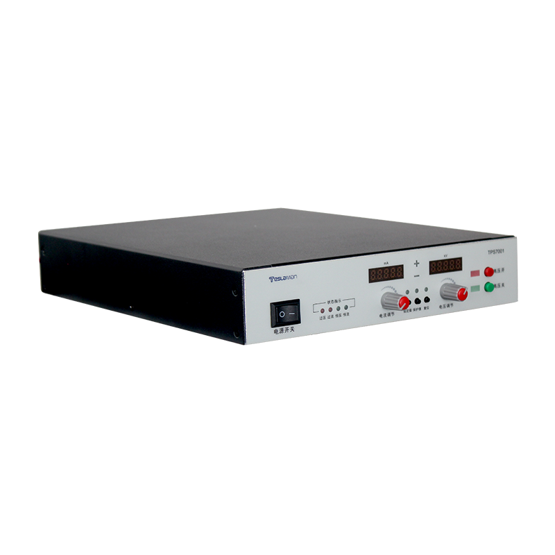
In the evolution of semiconductor manufacturing toward advanced process nodes of 7nm and below, the electrostatic chuck (ESC), as a core component for wafer clamping and precise positioning, has its performance stability directly determining the yield of key processes such as lithography and etching. The high-voltage power supply, serving as the energy core of the ESC, needs to continuously output a stable electric field to achieve damage-free wafer clamping. However, the existence of the dielectric interface trap effect often leads to electric field distortion and unbalanced charge accumulation, becoming a core bottleneck restricting the performance improvement of the ESC.
The essence of the dielectric interface trap effect is the trapping and release process of carriers by defect states (including dangling bonds, impurity energy levels, oxygen vacancies, etc.) at the interface between the ESC dielectric layer (e.g., Al₂O₃, SiO₂ composite layer) and the electrode/wafer. When the high-voltage power supply outputs voltage, some carriers are trapped by interface traps to form a space charge region, which not only weakens the intensity of the effective clamping electric field but also causes uneven electric field distribution. This is manifested in a clamping force difference of more than 15% between the edge and center of the wafer, further leading to problems such as wafer deviation and process pattern distortion. In addition, the long-term accumulation of trapped charges accelerates the aging of the dielectric layer and shortens the collaborative service life of the high-voltage power supply and the ESC.
To address this issue, a suppression system must be constructed from three dimensions: material optimization, power supply design, and control algorithm. At the material level, preparing a densified dielectric layer through the atomic layer deposition (ALD) process can reduce the interface defect density by more than 40%; meanwhile, introducing doped ions such as Mg²+ and Y³+ can effectively inhibit the formation of oxygen vacancies and reduce the source of trap states. In terms of power supply topology design, replacing the traditional hard-switching topology with a resonant high-voltage topology can reduce switching noise by 25dB, avoiding the carrier trapping behavior triggered by high-frequency noise. At the control algorithm level, the application of the adaptive charge compensation algorithm is particularly critical: based on the capacitance coupling principle, this algorithm real-time monitors the interface charge density and dynamically adjusts the output waveform of the high-voltage power supply—optimizing the traditional square wave into a stepped wave. During the voltage rise phase, charges are injected slowly to allow time for the release of trap-state carriers, controlling the fluctuation range of the clamping force within ±1%.
From the perspective of application effects, the aforementioned suppression technologies have been verified in the 3D NAND etching process: with the optimized high-voltage power supply-ESC system, the wafer warpage is reduced from 5μm to 1.2μm, the line width deviation of the etched pattern is narrowed by 30%, and the process yield is increased by 8%-12%. This indicates that the effective suppression of the dielectric interface trap effect can not only unleash the performance potential of the high-voltage power supply but also provide key support for the stability of advanced semiconductor processes.
In the future, as technologies such as extreme ultraviolet (EUV) lithography place higher demands on ESC clamping accuracy, the trap effect suppression technology for high-voltage power supplies will move toward intelligent perception-active regulation. By integrating AI algorithms to predict the accumulation trend of trapped charges and adjusting power supply parameters in advance, the transition from passive suppression to active prevention will be realized, providing more reliable energy support for the refined development of semiconductor manufacturing.