Technical Characteristics and Application Value of Multi-Stage Dynamic Compensation Network for High-Voltage Power Supply in Ion Implantation
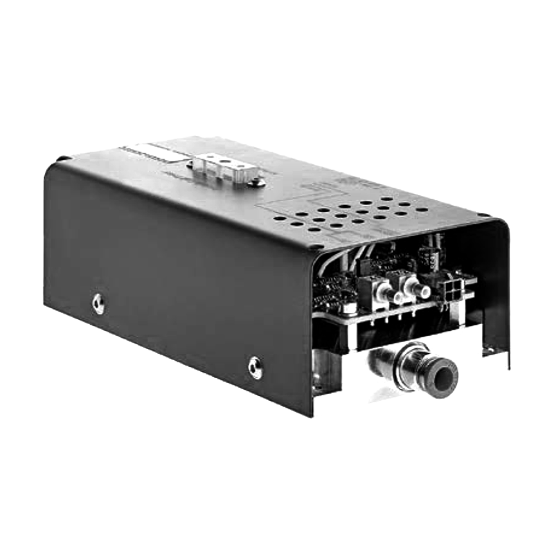
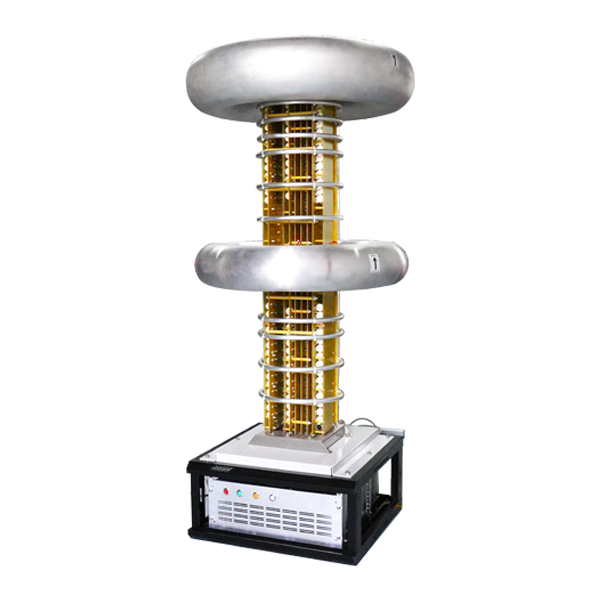
In advanced semiconductor manufacturing processes, ion implantation technology is the core process for achieving precise doping. Its strict requirements for doping dose uniformity and impurity depth control directly depend on the output stability of the high-voltage power supply (HVPS). The HVPS for ion implantation needs to provide high-voltage output ranging from kilovolts to megavolts. Under such operating conditions, factors like load disturbances (e.g., ion beam current fluctuations), grid ripple coupling, and device parameter drift easily cause the output voltage to fluctuate at the microvolt to millivolt level, thereby affecting implantation accuracy. To address this critical issue, the multi-stage dynamic compensation network (MSDCN) has become a core technological breakthrough direction in HVPS design. Through a layered and collaborative compensation mechanism, it achieves high-precision and stable control of high-voltage output.
The core architecture of the MSDCN is based on the layered control logic of prediction-real-time-correction and mainly consists of three functional modules. As a pre-adjustment unit, the feedforward compensation stage pre-sets compensation parameters under different beam current conditions by offline calibrating the load characteristic curve of the HVPS, thereby suppressing predictable disturbances (e.g., grid voltage fluctuations) in advance. This stage adopts a high-precision voltage reference and a parameter mapping algorithm, controlling the pre-response time of compensation at the microsecond level to prevent disturbances from propagating to the output terminal. The real-time feedback stage is the core of the compensation system. It realizes high-frequency sampling of the output voltage (with a sampling frequency up to 1 MHz or higher) through a high-voltage isolated sampling module. After the sampled signal undergoes differential amplification and noise suppression, it is transmitted to the digital control unit. The PID algorithm or model predictive control algorithm calculates the compensation amount, and then the high-speed power regulation unit realizes output correction. The response time of this stage can be as low as tens of nanoseconds, ensuring real-time suppression of sudden disturbances. Based on historical operating data and beam current variation trends, the load prediction stage uses machine learning algorithms to predict dynamic load changes (e.g., beam current mutations caused by ion source state switching) and adjusts the parameters of the feedforward and feedback stages in advance. This achieves the control effect of compensation preceding disturbance and solves the lag problem of traditional compensation networks.
In practical applications, the MSDCN needs to overcome two major technical challenges: first, the signal interference problem in high-voltage environments. The high-voltage electric field easily induces common-mode noise in sampled signals, affecting compensation accuracy. To solve this, the network adopts a design combining photoelectric isolation and differential sampling. It transmits sampled signals via optical fibers to isolate high-voltage electric field interference, while the differential structure suppresses common-mode noise, controlling the sampling error within 0.1%. Second, the coordinated control issue of multi-stage compensation. Improper parameter matching between stages may easily lead to compensation overshoot or oscillation. By introducing an adaptive coordination algorithm, the digital control unit can real-time optimize the gain and response speed of each stage, ensuring that the feedforward, feedback, and prediction stages complement rather than conflict with each other. For example, during the stable beam current phase, the role of the feedforward stage is enhanced to reduce power consumption; during the beam current mutation phase, the coordination between the feedback stage and the prediction stage is strengthened to improve response speed.
In terms of application value, this compensation network significantly improves the performance of the HVPS for ion implantation: it suppresses the output voltage ripple to below 5 mV (at 100 kV output) and increases the dose uniformity to within ±0.5%, meeting the doping requirements of advanced processes at 7 nm and below. Meanwhile, its wide load adaptability (covering a beam current range of 10 mA to 1000 mA) enables the power supply to be adapted to different types of ion implantation processes (e.g., shallow junction implantation, deep junction implantation), reducing the process switching cost of equipment. In addition, the digital design of the compensation network facilitates integration with the MES system in semiconductor manufacturing, enabling real-time monitoring and traceability of process parameters and providing data support for intelligent manufacturing.
In summary, through layered control and collaborative optimization, the MSDCN solves the stability problem of the HVPS for ion implantation. It not only improves the accuracy and consistency of the semiconductor doping process but also provides a new technical path for the application of HVPS in the field of precision manufacturing, promoting the technological upgrade of HVPS from high-voltage output to high-precision stable output.