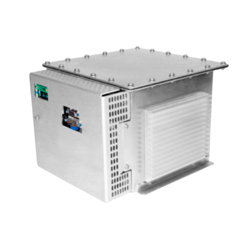
Load Mutation Response Strategy for High-Voltage Power Supply of Exposure Machine
When the exposure machine switches lithography processes (e.g., wafer batch replacement, pattern density change), the load of the high-voltage power supply will fluctuate suddenly (load rate jumps from 20% to 90% or vice versa), leading to output voltage overshoot (maximum deviation up to 10%) and current impact (peak value exceeding 1.5 times the rated value). This will not only cause lithography pattern line width deviation (exceeding 3nm) but also damage power devices (e.g., IGBT breakdown). The traditional response method uses fixed buffer resistors, which can suppress the impact but generate additional losses (accounting for more than 8% at heavy load) and cannot adapt to mutations of different amplitudes.
The load mutation response needs to be designed from the dual dimensions of "hardware buffering + software regulation": at the hardware level, a combined buffer circuit of "super capacitor + thyristor" is adopted. When the load rises suddenly, the super capacitor (capacity 1000F, withstand voltage 1000V) quickly releases electric energy to supplement the power supply output and suppress voltage drop; when the load drops suddenly, the thyristor is triggered to conduct, transferring excess energy to the energy-consuming resistor (made of alloy material, temperature resistance 1200℃) to avoid voltage overshoot. At the same time, the current transformer real-time monitors the impact current. When the current exceeds 1.2 times the rated value, hardware protection is triggered (response time <10μs); at the software level, the model predictive control (MPC) algorithm is used to predict the load mutation amplitude in advance by analyzing the load change trend in the previous 10ms (e.g., wafer pattern density distribution data). The PWM duty cycle of the power supply is adjusted 5ms before the mutation occurs, realizing advance intervention of "prediction-adjustment" and reducing the dynamic deviation after the mutation.
Through the test verification of a 193nm lithography exposure machine: when the load jumps from 30% to 85%, the voltage drop of the traditional scheme is 4.8% and the current impact is 1.4 times. After adopting the new strategy, the voltage drop is controlled within 1.2%, the current impact is reduced to 1.05 times, and the lithography line width deviation is reduced from 4.2nm to 1.8nm. At the same time, the buffer circuit loss is reduced from 8% to 2.5%, and the power supply efficiency is increased by 5.5%.