Energy Spatiotemporal Distribution Control of High-Voltage Power Supply for Ion Implantation
1. Process Requirements and Control Difficulties
Ion implantation is a core process for semiconductor doping. By accelerating specific ions (such as B, P, As) to an energy of 1keV-1MeV and implanting them into the wafer, a precise doped region is formed. The uneven energy spatiotemporal distribution will cause two major problems: first, the "temporal distribution unevenness" (voltage fluctuation) causes ion energy deviation, leading to a junction depth deviation of more than 5%; second, the "spatial distribution unevenness" (ion beam deflection) causes the difference in doping concentration between the edge and center of the wafer, affecting the performance consistency of transistors. For processes of 7nm and below, the ion energy stability needs to be controlled within ±0.1%, and the spatial distribution uniformity needs to reach ±2%.
2. Energy Spatiotemporal Distribution Control Technology
1.Closed-Loop Energy Feedback Control
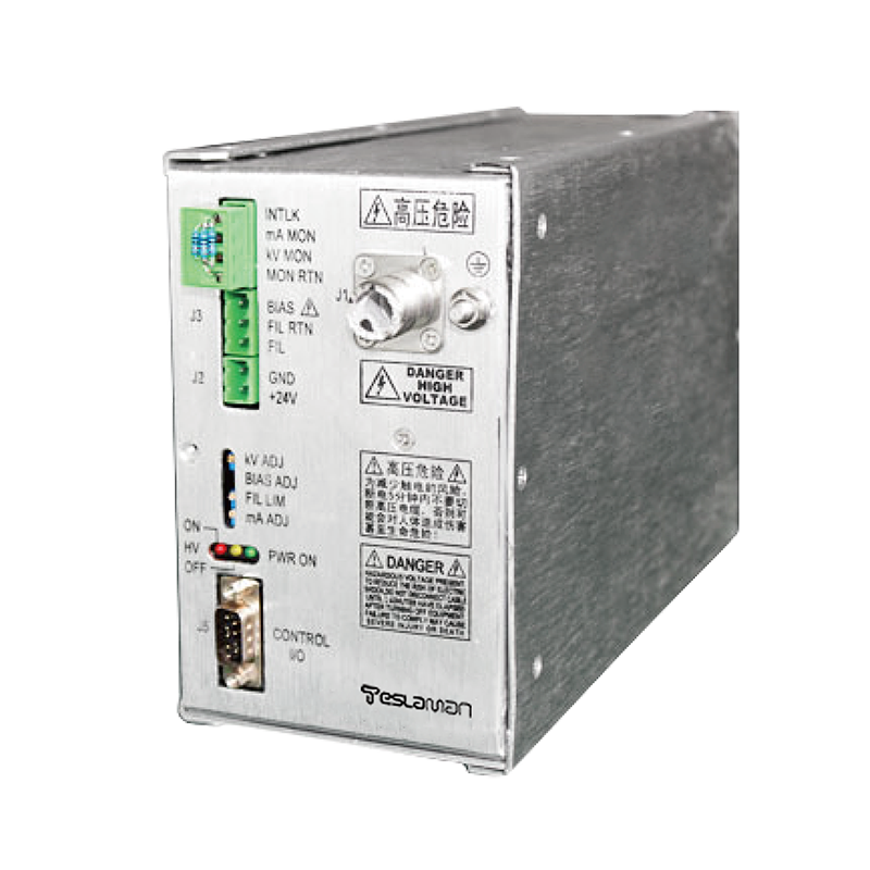
A high-precision energy analyzer (error < 0.001%) is connected in series at the output end of the power supply to collect the ion beam energy signal in real time and convert it into a voltage feedback value. Through the digital PID algorithm controlled by FPGA, the switching frequency of the high-frequency inversion module (50-200kHz) is adjusted to control the output voltage fluctuation within ±0.1%. At the same time, a two-stage structure of "pre-voltage stabilization + main voltage stabilization" is adopted. The front stage offsets the ±10% voltage fluctuation of the power grid, and the rear stage realizes fine adjustment.
1.Spatiotemporal Synchronization and Beam Current Compensation
In terms of timing control, clock synchronization technology is adopted to make the synchronization error of the high-voltage power supply, ion source trigger signal, and wafer scanning system less than 10ns, ensuring the precise matching between ion implantation timing and wafer movement; in terms of spatial control, the high-voltage power supply is linked with the voltage adjustment of the electrostatic lens. By monitoring the ion beam current at the wafer edge (accuracy 1nA), the focusing voltage of the electrostatic lens is dynamically adjusted to compensate for the energy loss of the ion beam at the wafer edge, so that the uniformity of ion energy distribution on the wafer surface reaches ±2%.
3. Process Application Effects
In the doping process of 7nm logic chips, the control scheme reduced the junction depth deviation at different positions of the wafer from 8% to 2%, and improved the doping concentration uniformity to ±1.5%; the difference in transistor leakage current was reduced to within 10%, and the switching speed stability was increased by 15%. The chip yield was increased from 75% to 90%, fully meeting the requirements of advanced semiconductor processes for ion implantation accuracy.