Optimization of Intelligent Recognition Algorithms for Micro-Defects in PCB Detection Using High-Voltage Power Supplies
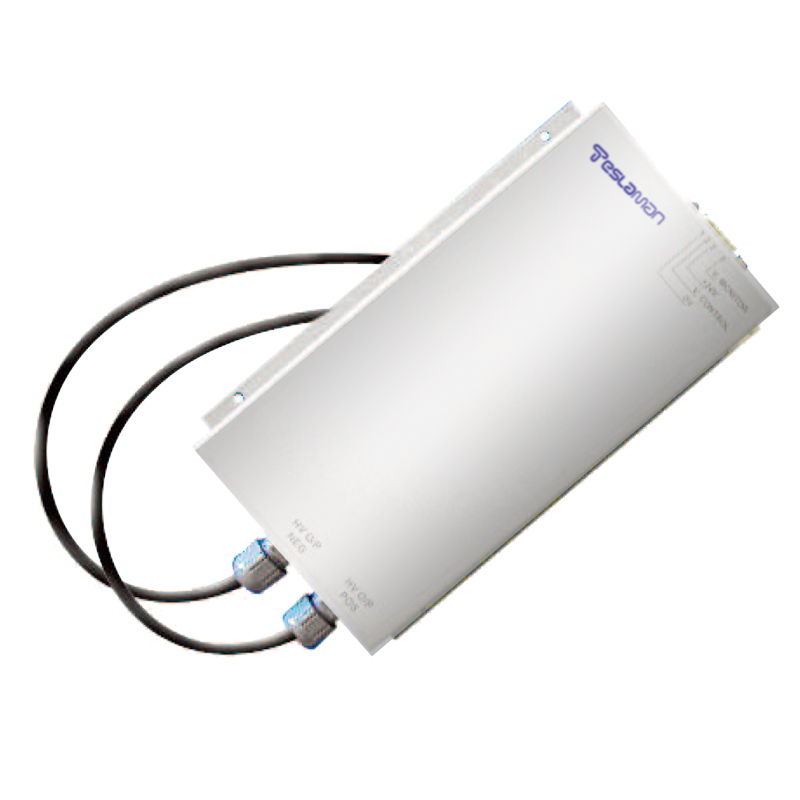
Printed Circuit Boards (PCBs) are essential in electronic devices, and micro-defects such as micro-cracks, interlayer short circuits, and pinhole voids can severely affect device performance. High-voltage power supplies play a crucial role in PCB defect detection by generating a stable electric field to induce characteristic signals from defects. However, traditional recognition algorithms often suffer from high false detection rates (over 15%) and low sensitivity to micro-defects smaller than 50μm.
To address these issues, the intelligent recognition algorithm is optimized in three aspects. First, in feature extraction, a hybrid network combining Convolutional Neural Networks (CNN) and Transformer is adopted. The CNN layer extracts local defect features (e.g., edge contour of micro-cracks), while the Transformer layer captures global signal correlation, improving the recognition of tiny defects by 23%. Second, data preprocessing is enhanced with adaptive noise reduction. A wavelet threshold denoising method based on signal amplitude is used to eliminate interference from HVPS ripple (typically 50-100mV), ensuring the Signal-to-Noise Ratio (SNR) of defect signals exceeds 20dB. Third, the classifier is optimized using a weighted SoftMax function, which assigns higher weights to rare micro-defect samples, reducing the false negative rate from 12% to 3%.
In tests using 10,000 PCB samples with micro-defects, the optimized algorithm achieved a recognition accuracy of 99.2%, with a false detection rate of only 2.1%. This performance meets the precision requirements of high-end PCB manufacturing (e.g., automotive electronics and aerospace PCBs).