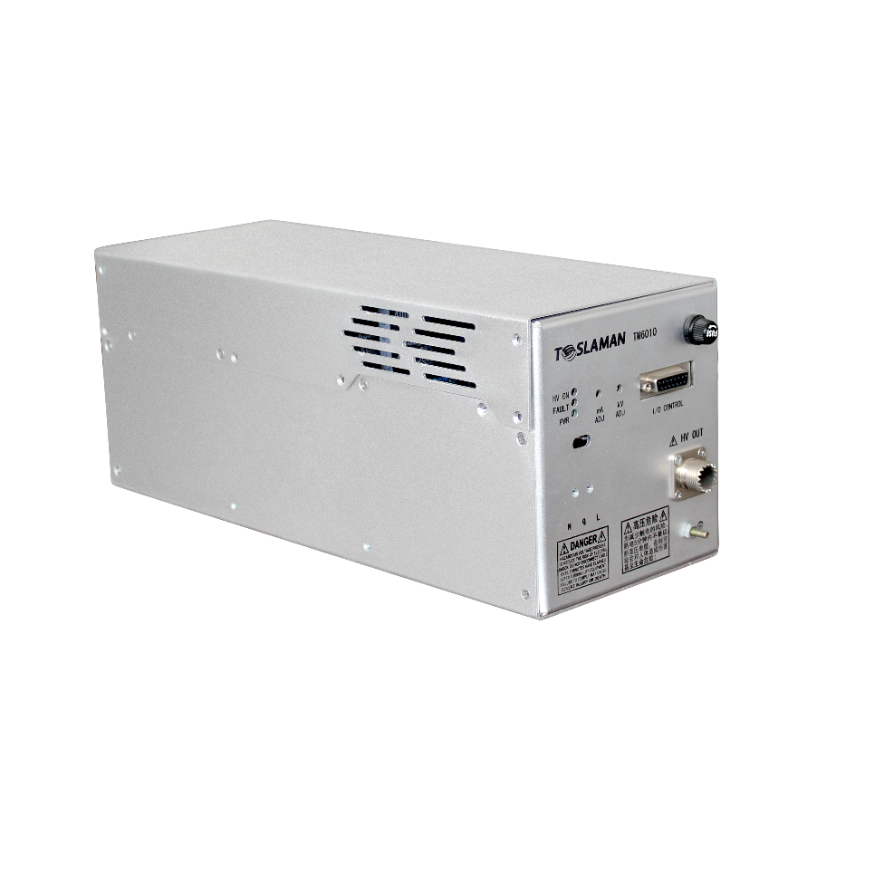
Precise Control of Ion Implantation Depth for High-Voltage Power Supplies in Ion Implanters
Ion implantation is a critical process in semiconductor manufacturing, used to dope impurities into silicon wafers to form functional regions (e.g., source and drain of transistors). The ion implantation depth is determined by the accelerating voltage of the ion implanter's high-voltage power supply, requiring a voltage control precision of ±0.1% to ensure depth accuracy (typically ±1% of the target depth). Traditional HVPS has difficulty meeting this requirement due to voltage drift and electromagnetic interference.
The precise control scheme for ion implantation depth includes three key technologies. First, a high-precision voltage reference is adopted. A bandgap voltage reference with a temperature coefficient of ±5ppm/°C provides a stable reference signal, reducing the impact of temperature on output voltage. Second, a dual-loop feedback control system is designed. The outer loop uses a high-accuracy voltage divider (ratio error ±0.005%) to sample the output voltage, and the inner loop samples the output current. The two loops work together to suppress voltage fluctuations caused by load changes (e.g., ion beam current variations) and external interference. Third, electromagnetic shielding and grounding optimization are implemented. The HVPS is enclosed in a copper shield (thickness 2mm) to reduce electromagnetic interference (EMI) from the ion implanter's vacuum system, and a star grounding topology is used to minimize ground loop noise, reducing voltage ripple caused by EMI to less than 0.03%.
In a 14nm semiconductor manufacturing test, the optimized HVPS achieved an accelerating voltage control precision of ±0.08%, and the ion implantation depth deviation was reduced from ±3.5% to ±0.8%, meeting the requirements of advanced semiconductor processes.