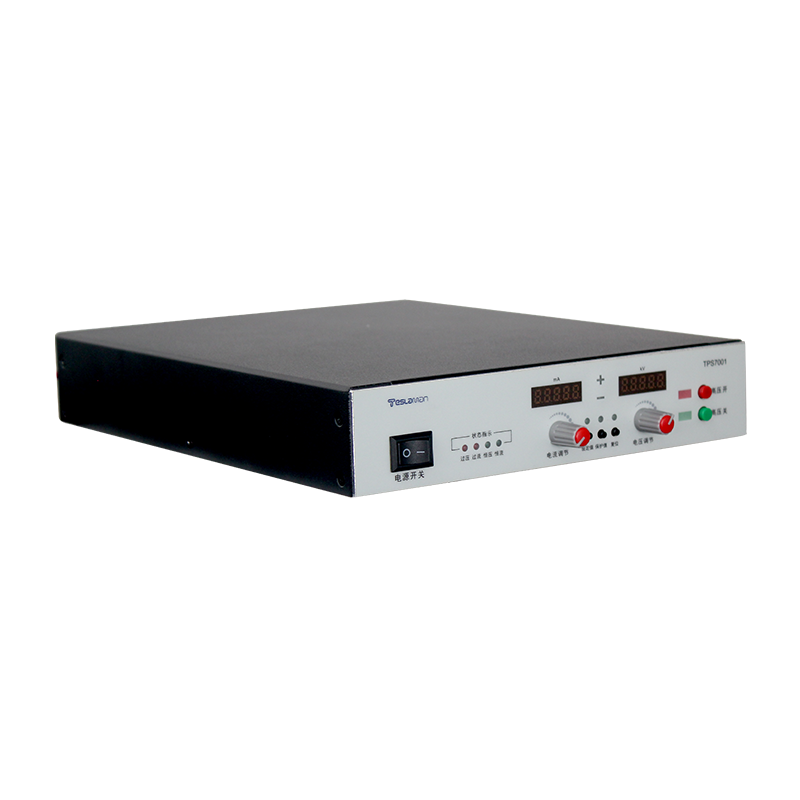
High-Voltage Power-Driven Process Optimization in Wafer Cleaning Systems
High-voltage power systems are central to the advanced wafer-cleaning processes used throughout semiconductor manufacturing, particularly as device geometries shrink and surface contamination tolerance approaches the atomic scale. Modern wafer-cleaning tools employ a variety of high-voltage mechanisms—including electrostatic deionization, charged-particle neutralization, high-voltage spray modulation, and plasma-assisted cleaning—to remove particulates, organic residues, ionic contaminants, and micro-pattern defects. Optimizing these processes requires high-voltage supplies that deliver exceptional stability, fast transient response, and adaptive waveform control tailored to diverse cleaning chemistries and surface conditions.
One of the most impactful applications of high-voltage power in wafer cleaning is electrostatic charge management. During chemical or mechanical cleaning processes, wafers can accumulate charge due to friction, turbulent fluid flow, or plasma exposure. Excess charge attracts particles, increases pattern sensitivity, and creates risk for line-edge roughness during subsequent lithography steps. High-voltage neutralization systems generate ionized fields that neutralize surface charge, ensuring stable electrostatic conditions. Optimization comes from delivering ultra-stable high-voltage output with minimal ripple so that ion density remains uniform across the wafer. Enhanced waveform linearity prevents ion bursts that could over-neutralize specific areas and introduce new electrostatic gradients.
High-voltage systems also support spray and jet-based cleaning mechanisms. In advanced cleaning chambers, high-voltage excitation modulates droplet size, charge distribution, and spray velocity. These parameters influence how cleaning solutions penetrate trenches, contact high-aspect-ratio features, and remove sub-nanometer residues. Optimized high-voltage pulse control—characterized by consistent rise time, tight voltage tolerance, and microsecond-level pulse precision—improves droplet uniformity and enhances cleaning penetration without damaging sensitive device structures.
Plasma-enhanced cleaning processes likewise rely heavily on high-voltage output. Low-damage plasma modes used for post-etch polymer removal or surface activation require stable high-voltage ignition and low-energy plasma sustainment. The power supply must handle rapidly shifting plasma impedance during gas transition, chamber pressure changes, and residue breakdown. Advanced digital control algorithms, wide-bandgap conversion stages, and adaptive pulse modulation help maintain a steady plasma density suited for fine-feature cleaning. This stability reduces over-etching risk and improves reproducibility across different wafer geometries.
Another important aspect is controlling high-voltage electrostatic chuck systems used during cleaning steps. As wafers are clamped for rotating and moving operations, high-voltage fields must remain uniform and stable to prevent micro-movements that could influence cleaning uniformity. High-voltage supplies equipped with rapid transient compensation, low leakage characteristics, and precise field-distribution control improve wafer stability, ensuring consistent mechanical exposure to sprays, brushes, or plasma zones.
Optimizing energy transfer efficiency also plays a role in improving cleaning performance. High-voltage conversion losses generate heat that can influence chamber temperature, fluid viscosity, and sensor stability. By improving conversion efficiency through resonant topologies, low-loss magnetics, and high-frequency switching, the system reduces thermal load and ensures consistent chemical and mechanical cleaning conditions. Stable thermal environments prevent deviation in fluid dynamics and chemical reaction rates, which are critical for removing sub-micron contamination across patterned surfaces.
Electromagnetic interference control contributes significantly to cleaning-process optimization. Wafer-cleaning equipment integrates optical sensors, contact-angle measurement units, particle counters, and flow sensors. High-voltage switching noise can interfere with these systems, degrading process control precision. By employing balanced switching waveforms, advanced shielding, and multi-layer filtering, high-voltage supplies maintain a clean electromagnetic environment. This ensures high measurement accuracy and supports real-time closed-loop process adjustments.
Diagnostics and predictive maintenance further enhance cleaning optimization. High-voltage modules that monitor switching stress, arc events, thermal drift, and output ripple can identify declining performance before it affects wafer quality. Predictive analytics enable targeted maintenance schedules that avoid sudden tool failures and reduce defect rates linked to electrical instability.
In addition, adaptive waveform generation is becoming a key enabler of cleaning performance. As wafer materials become more diverse—with porous low-k dielectrics, metal-hardmask layers, and fragile fin structures—cleaning recipes must adjust dynamically. High-voltage supplies capable of modifying pulse shape, frequency, and amplitude on demand allow cleaning tools to tailor treatment intensity to specific surface conditions. This reduces mechanical damage and chemical overexposure while maximizing residue removal efficiency.
Through improvements in high-voltage stability, waveform precision, EMI suppression, efficiency, and process-adaptive intelligence, high-voltage power systems significantly elevate wafer-cleaning consistency, throughput, and defect reduction.