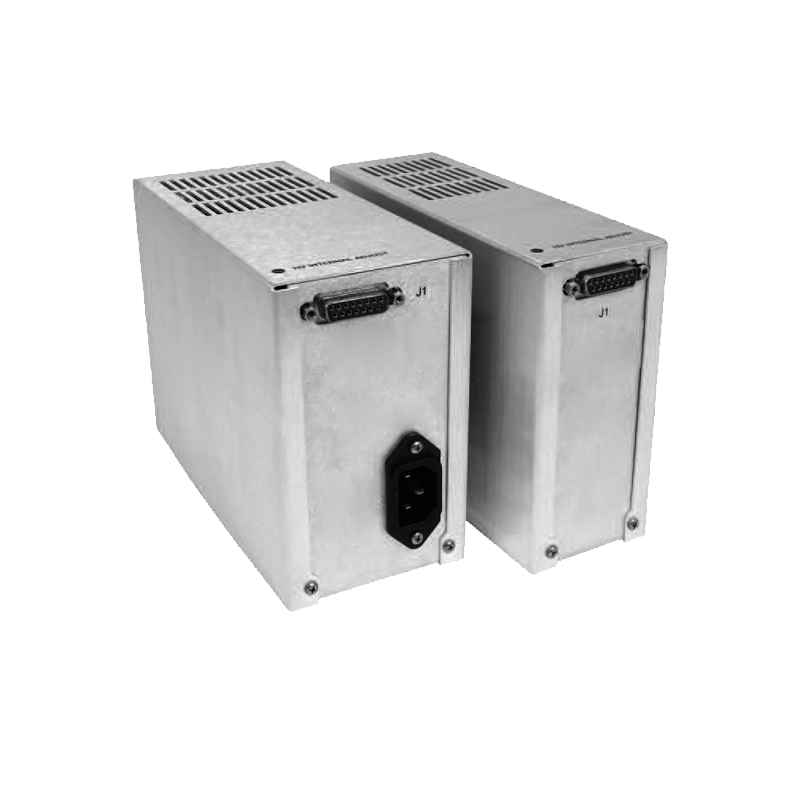
Lithography Equipment Power Capacity and Efficiency Dual Enhancement
The quest for continued feature size reduction in semiconductor manufacturing places lithography equipment at the epicenter of extraordinary power demands. Advancing technology nodes, particularly with the transition to Extreme Ultraviolet (EUV) and future High-NA EUV, necessitate a simultaneous enhancement of both power capacity and energy efficiency to ensure both high throughput and economically sustainable operation in high-volume manufacturing (HVM) facilities. The power system of a lithography tool is no longer a passive utility but an active determinant of the machine’s capacity (wafers per hour) and its operational efficiency (power consumption per wafer).
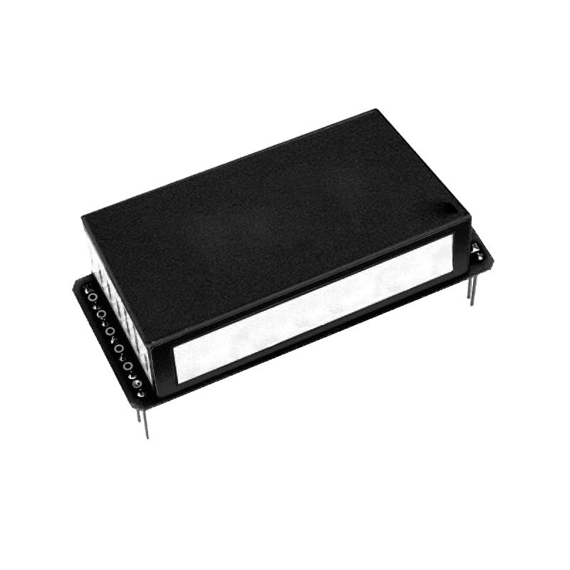
Increasing the lithography equipment's capacity is fundamentally linked to the ability of its power system to drive the light source at higher power and repetition rates, while simultaneously accelerating the wafer and reticle stages. For EUV, the target throughput of over 200 wafers per hour mandates light sources capable of 500 Watts or more of EUV output, which translates to gigawatts of peak electrical power consumption for the laser drivers and associated high-voltage systems. The power capacity enhancement is achieved through massive electrical infrastructure within the tool, utilizing ultra-fast charging circuits, large-scale capacitor banks, and high-current transmission lines engineered to handle the intense, pulsed power transients. Innovations in power architecture, such as multi-phase power delivery and the use of advanced power factor correction (PFC) stages, are critical to ensuring that the tool draws clean, stable power from the facility grid, minimizing line losses and maximizing the energy available for the light generation process. This sheer increase in power handling capacity is the direct enabler of the high-speed operation required for HVM throughput.
However, the pursuit of capacity cannot come at the expense of energy efficiency, which has become a significant economic and environmental concern for fabrication plants. The power consumption of modern lithography tools is substantial, making power-per-wafer a key metric. Efficiency enhancement focuses on minimizing parasitic power losses across all major subsystems. In the light source, this involves optimizing the conversion efficiency of the electrical energy into the desired EUV light. Advanced HV power topologies, employing resonance techniques and minimizing resistive losses, are designed to deliver energy to the plasma with the highest possible fidelity and least heat generation. Furthermore, the efficiency of the massive ancillary systems—including vacuum pumps, cryocoolers for thermal stabilization, and powerful motion control servos—must be optimized. This involves integrating intelligent, variable-speed drives and employing advanced energy recovery techniques, such as regenerative braking on the high-acceleration wafer stages, where kinetic energy is captured and returned to the power bus rather than being dissipated as heat.
The dual enhancement of capacity and efficiency requires a highly integrated and intelligent power management system. Modern lithography tools employ system-wide power telemetry and control. Sensors continuously monitor the power consumption, thermal profile, and efficiency of hundreds of internal power conversion points. Sophisticated algorithms use this data to dynamically adjust operating parameters. For example, during idle periods or non-critical process steps, power can be temporarily reduced to ancillary systems without impacting readiness. By carefully balancing the immense capacity required for maximum throughput with the imperative for high energy efficiency, power system engineering transforms raw electrical input into the precise, stable, and high-volume energy delivery necessary to make advanced semiconductor manufacturing both technologically feasible and economically viable. This optimization is the unsung engine driving the industry's scaling roadmap.