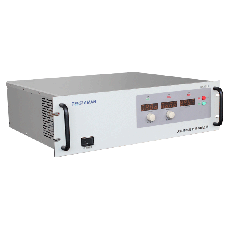
High-Voltage Power Supply Optimization for CMP Process Efficiency
The efficiency of chemical mechanical polishing processes hinges on precise control of electrostatic chucking forces, where even minor fluctuations in applied high-voltage can translate directly into removal rate variability, within-wafer nonuniformity, and edge yield loss. Optimization of high-voltage power delivery therefore targets three primary levers: minimization of energy dissipation during retention, acceleration of wafer handling sequences through faster charge and discharge cycles, and adaptive voltage profiling that aligns chucking force exactly with instantaneous process requirements.
Traditional fixed-voltage supplies maintain constant output throughout the entire polish cycle regardless of whether maximum retention force is needed. Optimized systems instead implement dynamic voltage scaling that references real-time downforce, platen rotation speed, and retaining ring pressure data to compute the minimum voltage required for stable wafer containment at every instant. In oxide polishing steps where downforce may vary from 4 psi during conditioning to under 1 psi near endpoint, this can reduce average chucking voltage by 35-45% while preserving margin against slip events. The resulting power savings compound across hundreds of wafers per day in high-volume lines.
Charge time represents another significant efficiency bottleneck. Legacy supplies using resistive charging paths require several seconds to reach target voltage, forcing extended dwell periods at the load station that limit overall throughput. Modern resonant conversion topologies combined with active gate drive optimization achieve rise times below 200 milliseconds even at 2000 V, enabling near-instantaneous chucking that supports sub-20 second wafer exchange cycles in the latest high-productivity platforms. Equally important is controlled discharge: active energy recovery circuits extract stored capacitive charge in under 100 milliseconds and return it to the DC bus at greater than 92% efficiency, eliminating the traditional bleed resistor losses that can exceed several watts continuously.
Multi-zone chucking optimization has emerged as a powerful efficiency multiplier. Independent high-voltage channels for inner, middle, and outer zones permit selective deactivation of regions experiencing minimal removal, particularly during profile correction steps where center-fast or edge-fast tuning is applied. By disabling up to 60% of total chuck area during certain phases, overall power drops proportionally while maintaining full retention force where material removal actually occurs. Cross-channel leakage compensation algorithms prevent voltage sagging in active zones caused by current draw in partially depowered neighboring zones.
Temperature-aware voltage adjustment addresses thermal effects on dielectric constant and backside gas conductivity. As wafer temperature rises during polishing, effective chucking force increases for a given voltage due to reduced helium ionization. Optimized supplies incorporate infrared wafer temperature measurements to reduce applied voltage in real time, preventing over-clamping that exacerbates edge rollover while harvesting additional energy savings.
Arc-free operation during voltage transitions demands sophisticated waveform shaping. Optimized systems employ S-curve trajectories that follow the dielectric strength envelope, avoiding field concentrations that trigger partial discharges. This not only improves energy efficiency by eliminating recovery delays after arc events but also extends dielectric lifespan by reducing cumulative stress.
Integration with endpoint systems enables anticipatory voltage reduction. As in-situ metrology detects approach to target thickness, the power supply begins gradual voltage ramp-down synchronized with downforce reduction, ensuring the wafer is already partially de-chucked when the platen stops. This eliminates the separate de-chuck step entirely in many processes, shaving valuable seconds from total cycle time.
Leakage current monitoring at picoampere resolution provides early warning of slurry ingress or dielectric degradation, allowing the system to increase voltage marginally to compensate rather than triggering full alarm states that halt production. This closed-loop compensation maintains process efficiency even as consumables age.
The combined impact of these optimizations routinely delivers 50-70% reduction in high-voltage subsystem energy consumption while simultaneously increasing wafer-per-hour throughput by 15-25% through shortened handling sequences, demonstrating that power supply refinement remains one of the highest-return efficiency investments available in mature CMP processes.