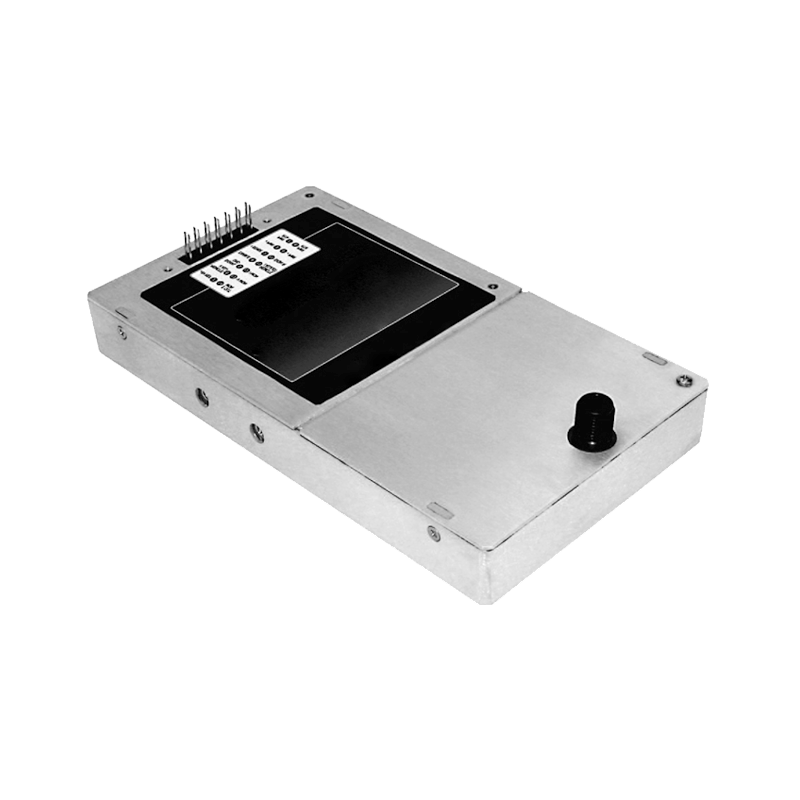
Fast-Discharge High-Voltage Module Design for Electrostatic Chucks
Electrostatic chucks in 300 mm plasma etch and deposition tools must clamp wafers with forces exceeding 50 Torr-liter while releasing them in under 400 ms to meet aggressive wafer-exchange targets of high-productivity cluster platforms. Fast-discharge high-voltage modules therefore operate in the ±800 V to ±2500 V range but are optimized primarily for controlled, ultra-low-energy residual charge removal rather than raw clamping power.
The discharge topology uses a bidirectional resonant converter capable of sourcing and sinking greater than 80 A peak current into the chuck capacitance of 8–25 nF. Active discharge occurs through a half-bridge of wide-bandgap gallium nitride transistors that drive a 1:1 air-core transformer directly coupled to the chuck electrodes via vacuum feedthroughs. Energy recovery efficiency exceeds 96 %, returning stored charge to the intermediate 400 V bus instead of dissipating it as heat.
Discharge waveform shaping is critical to prevent voltage rebound and particle launch. The module executes a three-phase sequence: first a constant-current sink at 60–75 A that collapses voltage exponentially to below 15 V in 120–180 ms; second a damped sinusoidal ringing phase that drives the remaining charge through zero and into slight opposite polarity; finally a low-bandwidth linear regulator that actively holds the electrodes at exactly 0.0 ± 0.3 V until the next clamp cycle. Total residual charge falls below 6 nC, corresponding to surface potential under 1 V across the wafer.
Charge neutralization accuracy is maintained by continuous monitoring of actual electrode current via coaxial shunt resistors with picocoulomb resolution. A digital PID loop adjusts discharge current amplitude and duration on every cycle to compensate for dielectric absorption and leakage variations caused by wafer backside helium flow changes or polymer deposition on the chuck surface.
Multi-zone chucks with up to 24 independent electrodes are supported by stacking identical discharge modules on a common backplane with fiber-optic isolation. Zone-to-zone timing stagger of 8 ms prevents mutual coupling through the wafer bulk silicon, eliminating the voltage bounce that previously caused placement errors greater than 80 µm in extreme cases.
Safety circuitry incorporates dual independent current-limit thresholds: a fast analog comparator that disables gate drive within 800 ns of detecting overcurrent indicative of chuck-to-wafer arcing, and a slower digital monitor that flags excessive integrated charge transfer suggestive of dielectric puncture. Both paths force immediate transition to a high-impedance state and assert a hardware interlock that requires manual reset.
Thermal design uses immersion cooling in fluorinated fluid with boiling point above 120 °C, allowing peak discharge currents without local hotspots while maintaining junction temperatures below 65 °C even during continuous 20-wafer-per-minute cycling. The absence of electrolytic capacitors and optocouplers further enhances reliability in the aggressive fluorine and chlorine environments of advanced etch chambers.
These fast-discharge modules routinely achieve full de-chuck in 280–350 ms with residual surface potential below 0.6 V, enabling robot end-effector entry speeds above 500 mm/s and contributing directly to wafer exchange contributions under 4.5 seconds in the most advanced 3 nm etch platforms.
