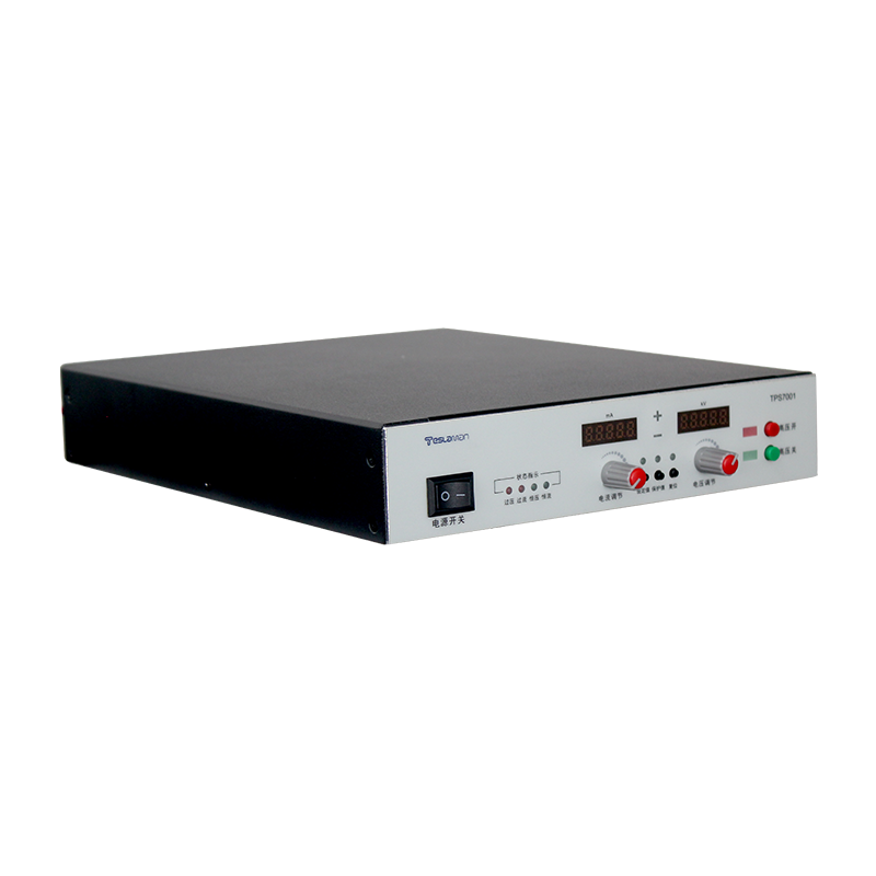
RF Matching High-Voltage Bias Supply for Ion Beam Etching Systems
Precision ion beam etching of compound semiconductor devices and X-ray optics demands 100–1500 eV argon ions with energy spread below 1.8 eV FWHM, requiring a bias supply capable of 200–1500 V DC superimposed on 13.56 MHz RF up to 600 W while automatically maintaining match across widely varying plasma impedance presented by changing target materials.
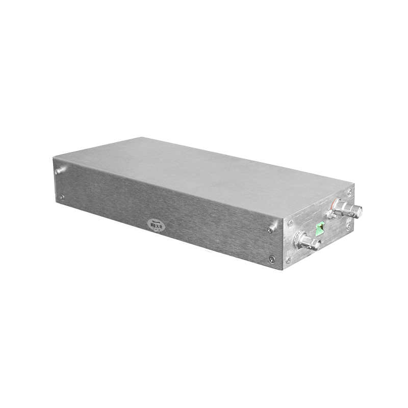
The hybrid supply uses a linear Class-A MOSFET amplifier for the DC bias component capable of sourcing/sinking 1.2 A continuously, paralleled with a solid-state RF injector using dual laterally-diffused MOSFETs in push-pull configuration. Both sections are coupled to the substrate electrode through a shared vacuum capacitor matching network that presents low impedance to DC and precisely 50 Ω to RF.
Impedance matching is performed by a digital RF vector matching algorithm operating at 28 kS/s that controls two vacuum variable capacitors via piezoelectric motors. Reflected power is held below 1.8 W by continuously adjusting load capacitance and tuning inductance with 0.6 fF and 22 pH resolution respectively. Match acquisition time after target change is under 480 ms.
Bias voltage regulation during RF coupling uses active ripple cancellation: a sense winding on the RF transformer drives a counter-phase injection amplifier that nulls 13.56 MHz modulation to below 180 mV p-p at the wafer. DC regulation remains within ±0.6 V even during 400 W to 40 W power steps.
Beam energy purity is protected by a fast overcurrent clamp that limits substrate current to 110 % of setpoint within 800 ns, preventing acceleration of secondary ions during momentary arcs. Recovery implements a soft-start ramp over 22 ms to avoid ringing the matching network.
Thermal management uses chilled water cooling plates bonded directly to the MOSFET heat spreaders, maintaining case temperature within ±1.1 °C across full power envelope. All control electronics are fiber-isolated from the high-voltage electrode to eliminate ground loops that previously caused etch rate drift of 0.9 % across 200 mm substrates.
These RF-matched bias supplies routinely deliver ion energy distribution with <1.4 eV FWHM at 1200 eV while maintaining etch rate uniformity below 1.1 % non-uniformity on 150 mm GaAs and fused silica optics, enabling surface roughness below 0.18 nm RMS after 800 nm material removal.