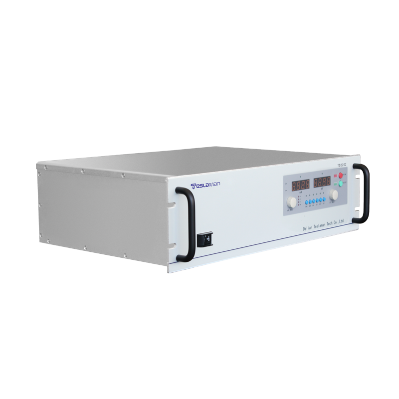
Capacitive Charging Power Supply Resonant Topology Optimization
Capacitive loads, ranging from pulsed power systems and defibrillators to electromagnetic launchers and laser flashlamps, present a unique set of challenges for high-voltage power supplies. The fundamental task is to transfer energy from a primary source to a capacitor bank efficiently and rapidly, often with stringent requirements on charge time consistency, voltage accuracy, and component stress. Traditional charging methods using linear regulators or hard-switched converters suffer from excessive losses, thermal stress, and electromagnetic interference at the power levels required. This has driven the widespread adoption and continuous optimization of resonant converter topologies for capacitive charging applications, where the goal is to align the converter's natural dynamics with the load characteristics for near-lossless operation.
The core advantage of a resonant topology lies in its ability to shape the current and voltage waveforms through the careful interplay of inductors and capacitors, enabling zero-current switching (ZCS) or zero-voltage switching (ZVS) of the semiconductor devices. For capacitive charging, the series resonant converter (SRC) and the parallel resonant converter (PRC), along with their hybrid variants like the series-parallel resonant converter (SPRC) or LLC converter, are the primary candidates. The optimization process begins with a detailed modeling of the load. A capacitive bank is not a simple fixed capacitor; it possesses equivalent series resistance (ESR) and inductance (ESL). Furthermore, during the charge cycle, its terminal voltage rises linearly with stored charge, meaning the effective load impedance seen by the supply changes dramatically from a near-short circuit at the start of charge to a high impedance at the target voltage.
For a series resonant converter, the resonant inductor and capacitor are placed in series with the transformer leakage inductance and the load. This topology inherently limits the inrush current at the start of charge due to the series impedance, providing a natural soft-start. Optimization focuses on selecting the resonant frequency relative to the switching frequency and the characteristic impedance of the resonant tank. Operating above the resonant frequency (inductive region) is often preferred to ensure ZVS for the primary-side switches, reducing turn-on losses. The tank's characteristic impedance, defined by sqrt(Lr/Cr), must be chosen to limit the peak current through the switches and transformer while still delivering the required power. Mathematical modeling using state-plane analysis or extended describing functions is crucial to predict the trajectory of the resonant tank states (inductor current, capacitor voltage) throughout the charge cycle, ensuring the converter remains in a stable, controllable mode from empty capacitor to full voltage.
The parallel resonant converter, where the resonant capacitor is in parallel with the load, presents a different set of characteristics. It acts as a nearly constant current source over a wide load range, which is beneficial for charging. However, it can suffer from high circulating currents and requires switches capable of handling high peak voltages. Optimization here often involves hybrid approaches. The LLC resonant converter, featuring a resonant inductor, a magnetizing inductor, and a resonant capacitor, has gained significant traction. Its gain characteristic is a function of switching frequency and load. By frequency modulation, the converter can maintain high efficiency across the entire charging profile. At the beginning of charge (low load impedance, equivalent to a high load condition), the converter operates at a frequency well above resonance, providing limited gain and current. As the capacitor voltage rises (increasing load impedance), the switching frequency is swept down towards resonance, increasing the gain to continue pushing energy into the now higher-voltage load. This frequency sweep is a key control optimization, often managed by a digital signal controller that continuously solves the resonant tank equations in real-time or references pre-calculated look-up tables.
Beyond the topological choice and component sizing, practical optimization encompasses every aspect of the design. The high-voltage transformer is a centerpiece. Its leakage inductance is often incorporated as part of the resonant inductance, requiring tight control over its value during manufacture. Interwinding capacitance must be minimized to prevent high-frequency bypass of the resonant network. The selection of switching devices, typically silicon MOSFETs or IGBTs for medium frequency, or silicon carbide MOSFETs for higher frequencies, is dictated by the resonant voltage and current stresses, which differ markedly from square-wave converters. Gate drive circuits must be optimized for speed and isolation to maintain precise timing at high frequencies. Furthermore, closed-loop control is essential for final voltage accuracy. A constant current or constant power charge profile is typically commanded. A feedback loop measures the capacitor voltage, often through a high-resistance divider and isolation amplifier, and adjusts the switching frequency or phase-shift modulation accordingly to terminate charge precisely at the setpoint, minimizing overshoot. The ultimate measure of optimization is the achieved combination of charge time, efficiency across the entire cycle, thermal performance, component stress margins, and reliability over millions of charge-discharge cycles.