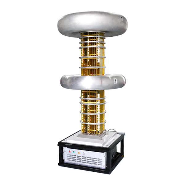
Ion Implantation Wafer Bow Compensation Power Supply
Ion implantation is a standard process for introducing dopants into semiconductor wafers. High-dose implants, particularly those used for forming wells, buried layers, or in advanced packaging technologies, can induce significant stress in the silicon crystal lattice. This stress manifests as wafer bow or warp, a curvature that can lead to severe downstream problems in photolithography (defocus, poor overlay), handling (robot arm collisions, chucking issues), and overall yield loss. While process-level optimizations exist, an in-situ electromechanical approach to actively control bow during the implant process itself has emerged, relying on specialized electrostatic or thermal chucking systems driven by sophisticated power supplies. This discussion explores the requirements for high-voltage and high-current power supplies used in active wafer bow compensation during ion implantation.
The underlying cause of bow is the asymmetry of the implant-induced stress. Ions penetrating the wafer surface create a damaged, strained layer. If this layer is not symmetric through the wafer's thickness—due to a single-sided implant—the wafer bends, much like a bimetallic strip. Compensation strategies aim to counteract this bending force in real-time. The two primary active methods involve either an electrostatic chuck (ESC) capable of applying localized clamping forces or a thermal chuck designed to create a compensating thermal gradient.
In an electrostatic chuck-based compensation system, the wafer is held not by a uniform vacuum, but by a multi-zone ESC. Each zone, typically arranged in concentric rings or a matrix, can have its clamping voltage independently controlled. The clamping force is proportional to the square of the applied voltage. By modulating the voltage on different zones, one can apply a differential clamping force across the wafer backside. To counteract an implant-induced bow that would make the wafer convex on the implant side, one would increase the clamping force on the central zones relative to the edge, effectively pulling the center of the wafer down more firmly and flattening it. This requires a multi-channel high-voltage power supply system. Each channel must provide a stable, programmable DC voltage, typically in the range of 500V to 3kV, depending on the ESC design and the required force. The critical requirement is the ability to modulate these voltages smoothly and dynamically during the implant scan. As the ion beam scans across the wafer, the stress profile evolves. A pre-programmed voltage profile for each chuck zone can be executed, but a closed-loop system is more robust. This would use in-situ wafer bow sensors, such as laser triangulation or capacitive gauges, to provide real-time feedback. The power supply control system must then adjust the multi-zone voltages using a control algorithm (e.g., a multi-input-multi-output PID controller) to null the measured bow. This demands power supplies with fast update rates, low noise (to prevent force jitter), and excellent channel-to-channel isolation to prevent cross-talk that could create instability.
The thermal compensation method operates on a different principle. By creating a controlled temperature gradient through the wafer thickness, one can induce a thermal stress that opposes the implant stress. This is often achieved using a multi-zone thermal chuck with independent heating and/or cooling elements. The power supply challenge here shifts from high voltage to high current and precise temperature control. Each zone requires a programmable, high-current driver for a resistive heater or a thermoelectric cooler (TEC). The magnitude of compensation is controlled by the temperature setpoint of each zone. To correct bow, the chuck would be programmed with a radial thermal profile—for example, cooling the center relative to the edge to create a convex thermal bow that counters a concave implant bow. The power supplies for these heaters/TECs must have precise, closed-loop temperature control, using feedback from embedded RTDs or thermocouples in each chuck zone. The control loop must account for the thermal mass of the chuck and wafer and the changing thermal load as the ion beam itself deposits significant energy (several kilowatts) into the wafer. This necessitates power supplies with high control bandwidth and the ability to source and sink current for TECs. The stability of the temperature control, often to within 0.1°C, directly translates into stability of the compensation stress.
Integration with the implanter presents significant challenges. The compensation system operates in the harsh environment of the implant end station: under high vacuum, subjected to stray ions and x-rays, and in the presence of strong magnetic fields from the beamline magnets. All power supply components and sensors must be designed to function reliably in this environment. Feedthroughs for multiple high-voltage or high-current lines must be carefully designed to prevent arcing and maintain vacuum integrity. Furthermore, the compensation system must not interfere with the primary implant process. For an ESC system, the varying clamping voltages must not modulate the wafer's electrical potential in a way that deflects the ion beam. Careful grounding and shielding schemes are essential. For a thermal system, the chuck design must not compromise the wafer's thermal conductivity in a way that leads to excessive implant temperature rise, which can cause dopant diffusion and defect annealing.
A hybrid approach is also feasible, using a combination of electrostatic force and thermal management. This would require an even more complex power supply system integrating both high-voltage multi-channel outputs and high-current thermal control outputs, all under a unified control algorithm that processes wafer bow sensor data.
In summary, wafer bow compensation power supplies are specialized systems for active substrate stabilization. They move beyond simple power delivery into the realm of real-time, multi-zone mechanical stress control. Whether based on electrostatic force or thermal gradients, they demand multi-channel programmability, fast closed-loop response, exceptional stability, and ruggedness for the implant environment. By actively countering implant-induced stress as it occurs, these systems enable the use of high-dose implants without compromising planarization, thereby improving overlay accuracy in subsequent lithography steps and increasing the yield for advanced semiconductor devices and 3D integration schemes.
