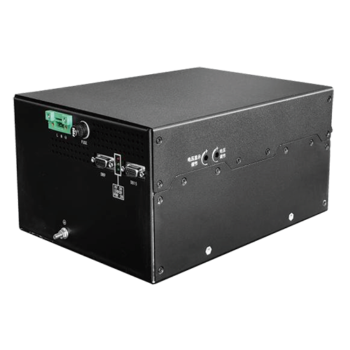
Coating Pulsed Power Supply for Plasma Density Modulation
In advanced thin film deposition, particularly using High Power Impulse Magnetron Sputtering (HiPIMS) and its derivatives, the pulsed power supply is the primary tool for controlling the ionization fraction and energy distribution of the sputtered material. Unlike DC sputtering where plasma parameters are in a steady-state equilibrium, pulsed operation creates a highly non-equilibrium, time-dependent plasma with distinct phases: a short, high-power pulse that generates an ultra-dense, highly ionized plasma plume, followed by a long off-time where the plasma decays and the target cools. By strategically modulating the pulse parameters, it is possible to exert unprecedented control over the plasma density and, consequently, the flux and energy of ions arriving at the substrate. This enables the engineering of film density, crystallographic orientation, and residual stress in ways impossible with DC.
The fundamental control variables of the pulsed power supply are the pulse waveform, voltage/current amplitude, pulse width (ton), and pulse repetition frequency (PRF). Plasma density modulation is achieved by manipulating these parameters to control the peak power density on the target and the temporal evolution of the discharge. During the initial phase of a pulse (tens of microseconds), a high voltage is applied to break down the gas and initiate the sputtering process. The current then rapidly rises as a dense plasma forms. The peak plasma density is directly correlated with the peak current, which is a function of the applied voltage, the gas pressure, and the magnetic field configuration. A power supply capable of delivering very high peak currents (hundreds of amperes to kiloamperes) from a moderate voltage (hundreds of volts) is essential for creating the high-density plasma characteristic of HiPIMS. This is typically achieved using a capacitor-based pulse-forming network (PFN) or a modern, switch-mode power supply with large output capacitors and very low internal impedance.
Precise modulation requires the supply to operate in distinct modes. For controlling the *magnitude* of the peak plasma density, the amplitude of the current pulse is key. This can be done by controlling the charge voltage on the PFN capacitors or by using a current-regulated switch-mode supply that clamps the current at a set peak value. However, true temporal *shaping* of the plasma density within a single pulse offers finer control. Advanced supplies can generate non-rectangular pulse shapes. For instance, a pulse with a fast-rising edge to quickly achieve a high plasma density, followed by a sustained plateau or a slowly decaying tail, can be used to separate the highly ionized metal flux (which arrives later in the pulse) from the initial neutral flux. This is achieved by real-time feedback control of the output switches, modulating voltage to maintain a desired current trajectory (e.g., constant current, or a specific current vs. time profile). This capability allows the process engineer to "sculpt" the ionization fraction over time.
Modulation of the plasma density *between* pulses is controlled by the PRF and duty cycle. A high PRF with a short off-time leads to a higher time-averaged plasma density, as the plasma does not fully decay between pulses. This is beneficial for increasing deposition rates but reduces the degree of ionization per pulse due to lower peak power. Conversely, a low PRF with a long off-time allows for complete plasma decay and target cooling, enabling extremely high peak power in the next pulse and thus a very high instantaneous ionization fraction, but at a lower average rate. The power supply must therefore offer a wide, stable range of PRF and duty cycle control, with precise synchronization to substrate bias pulses or other external triggers.
The interaction between the pulsed supply and the plasma load is highly dynamic and non-linear. The impedance of the magnetron changes dramatically during a pulse, from nearly infinite at breakdown, to a fraction of an ohm at peak current, and back. The power supply's control loop and output stage must be designed to remain stable across this entire range. Furthermore, to study and optimize these modulation schemes, the power supply needs to provide detailed real-time diagnostics, such as waveforms of voltage, current, and instantaneous power for each pulse. This data is used to correlate electrical input with plasma characteristics measured by Langmuir probes or optical emission spectroscopy.
Ultimately, the pulsed power supply for plasma density modulation is not just a power source but a waveform generator for material synthesis. By providing deterministic control over the time-history of plasma density and ionization, it allows the deposition process to be tailored at a fundamental level. This enables the growth of exceptionally dense, smooth coatings at low temperatures, the deposition of crystalline films without substrate heating, and the filling of high-aspect-ratio trenches with perfect conformality—key requirements in semiconductor metallization, wear-resistant tool coatings, and optical layer fabrication.