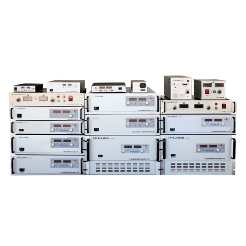
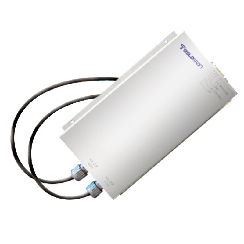
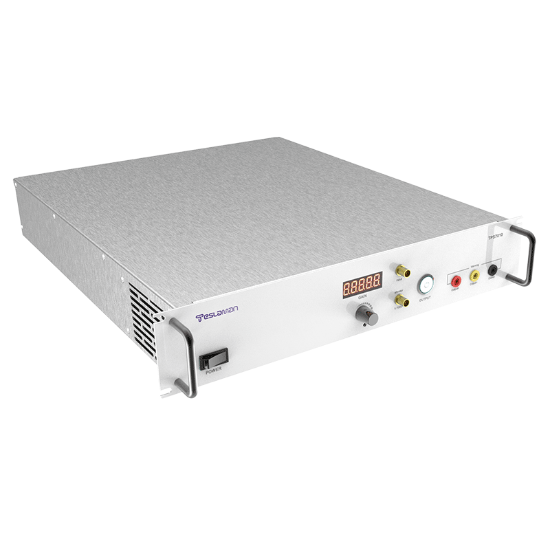
Ion Implantation Beam Profile Scanning Power Supply
In ion implantation for semiconductor manufacturing, achieving precise dopant profiles across a wafer requires meticulous control over the spatial distribution of the ion beam. The process of beam scanning, whereby the ion beam is systematically moved across the stationary wafer, is a primary method to ensure dose uniformity. The power supply systems responsible for driving the electromagnetic deflection elements that execute this scanning are critical components whose performance directly impacts implant angle accuracy, dose uniformity, and throughput. These scanning power supplies must deliver highly stable, precisely controlled currents to the scan coils or plates, translating digital patterning commands into flawless physical beam motion under dynamically changing load conditions.
The fundamental scanning architecture typically involves two orthogonal electromagnetic dipoles for horizontal (X) and vertical (Y) deflection. The power supplies driving these coils are high-precision, bipolar current sources. Their core requirement is exceptional linearity. The relationship between the commanded digital setpoint (from the implant controller's scan generator) and the actual magnetic field produced must be perfectly linear and identical for both axes. Any non-linearity introduces geometric distortion in the scan pattern; a designed raster pattern may become pin-cushioned or barrel-shaped, leading to localized dose non-uniformities. To achieve this, the amplifiers employ high-resolution digital-to-analog converters (DACs) for setpoint definition and use closed-loop feedback control based on direct current measurement via precision shunt resistors. Temperature compensation of all critical components is essential to maintain linearity over long operational periods.
Stability and low noise are equally paramount. The ion beam's position is proportional to the instantaneous current in the scan coils. Any ripple or random noise on this current causes the beam to jitter around its intended position. This jitter effectively blurs the dose profile, smearing out the intended sharp edges of implanted regions and degrading the accuracy of high-tilt angle implants. Therefore, scanning power supplies are designed with ultra-low noise output stages, often utilizing linear amplification for the final stage or sophisticated filtering in switched-mode designs. The power spectral density of the output noise, particularly in the frequency bands relevant to the scan speed, is a key specification. Furthermore, the long-term drift of the output current must be negligible over the time scale of a single wafer implant to prevent a gradual shift of the entire scan pattern.
The dynamic response of the system is tested during the turnaround points of the scan pattern. In a raster scan, the beam moves linearly across the wafer, then must rapidly "flyback" to start the next line. During this flyback period, the beam is typically blanked to prevent implantation. The speed of this retrace is limited by the slew rate of the scan amplifiers and the inductive nature of the coils. The amplifiers must provide sufficient voltage headroom (compliance voltage) to force the current change through the coil inductance (V = L di/dt). A slow flyback reduces throughput. More critically, the amplifiers must settle to the new precise current value for the start of the next scan line within a very short time. Overshoot, ringing, or slow settling at the line start would cause dose errors at the wafer's edge. This demands amplifiers with high bandwidth, optimal damping, and control algorithms that may include feedforward compensation based on the known inductive load.
A significant challenge is the changing load impedance presented by the scan coils. As the beam is deflected, the physical position of the coil within the implanter's magnetic environment changes, which can slightly alter its inductance and resistance due to eddy currents in nearby metallic structures. Additionally, the coils themselves heat during operation. A robust scanning power supply design must be insensitive to these modest load variations, maintaining its transfer function (current output vs. command) regardless. This often involves adaptive control loops or pre-characterization of the load across its operational range.
Synchronization with the entire implant system is a complex, deterministic timing exercise. The scan power supplies receive their setpoint updates from a master scan generator clock. This clock must be synchronized with the beam blanking signal (to gate the beam off during flyback) and with the mechanical scan of the wafer platen in hybrid scan systems. Any timing jitter in this synchronization chain causes placement errors. In advanced implanters, the scanning is not a simple raster but may involve variable velocity scanning, where the beam slows at the wafer edges to compensate for increased dwell time, requiring real-time modulation of the scan amplifier's slew rate based on position. This level of integration demands a digital interface with low latency and high data throughput between the scan controller and the power supplies.
For high-current implanters, space charge effects within the beam can cause beam blow-up, which interacts with the scanning process. Some systems employ dynamic focus correction, where the current in auxiliary focus coils (or even a component of the scan coil currents themselves) is adjusted in real-time as a function of beam position to keep the beam focused on the wafer plane. This requires the scan power supply system to have additional, coordinated control channels or to output a derived focus correction signal to a separate supply.
Finally, diagnostics and safety are integrated. The scan power supplies typically provide readback of actual output current and voltage. This data is used for closed-loop verification of the scan pattern and for fault detection. A failure mode where a scan amplifier loses control and drives the beam to a static position would result in catastrophic localized overdose and wafer destruction. Therefore, independent watchdog circuits monitor the commanded versus actual scan signals and will trigger a beam shutdown if a major discrepancy is detected. In summary, ion implantation beam scanning power supplies are high-fidelity, wide-bandwidth current amplifiers operating as the final actuators in a precision beam positioning loop. Their linearity, stability, speed, and synchronization fidelity are directly imprinted onto the dopant distribution within the silicon, influencing device performance, yield, and the ability to fabricate advanced semiconductor nodes.


