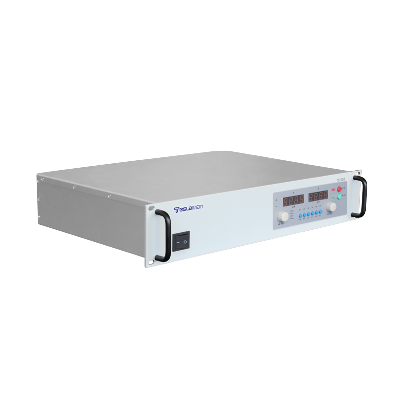
Ion Beam C leaning High Voltage Power Supply Parameter Optimization
Ion beam c leaning and surface modification is a precise technique used to remove contaminants, oxides, or thin layers from substrates prior to deposition, bonding, or analysis. The process involves directing a beam of inert gas ions (typically Ar+) from a broad-beam ion source onto a target surface in a vacuum chamber. The quality and effectiveness of the cleaning process—its uniformity, etch rate, and induced surface damage—are exquisitely sensitive to the parameters of the ion beam. These parameters are almost entirely controlled by the high-voltage power supply system that energizes the ion source. Therefore, parameter optimization is not a one-time calibration but a systematic exploration of the multi-dimensional space defined by the supply's outputs to identify the Pareto-optimal setpoints for a specific material and desired outcome.
The ion so urce, often a Kaufman-type or an inductively coupled plasma (ICP) source, requires multiple interdependent power supplies. The key parameters for optimization are: 1) Discharge Voltage/Current (Vd/Id): This controls the creation and density of the plasma within the source. Higher discharge power increases plasma density, which generally leads to a higher ion beam current. 2) Accelerator/Decelerator Grid Voltages (Vacc, Vdec): A multi-grid ion optical system extracts and focuses ions from the plasma. The negative accelerator grid voltage (Vacc, typically -100V to -1000V) defines the extraction field strength and the final ion energy. The decelerator grid voltage (often near ground or slightly positive) shapes the beam potential at the exit. The ratio and absolute values of these grid voltages are critical for determining the beam current density, divergence angle, and the fraction of electrons co-extracted to neutralize the beam. 3) Neutralizer Bias: A separate hot filament or plasma bridge neutralizer emits electrons into the beam to prevent charge buildup on insulating substrates. Its bias voltage relative to the chamber affects the beam's space charge compensation and, consequently, its focus and stability.
The optimi zation process is multi-objective and often conflicting. The primary objectives are: Maximizing Etch Rate, which demands high beam current density; Minimizing Surface Damage/Roughness, which requires lower ion energy and a well-collimated, uniform beam to avoid localized sputtering; and Achieving Maximum Uniformity across the substrate, which depends on beam optics and the source's plasma homogeneity. The power supply parameters directly trade off between these goals. For example, increasing the discharge current (Id) raises beam current, boosting etch rate. However, if the accelerator voltage (Vacc) is held constant, the increased plasma density can lead to increased space charge effects in the extraction region, causing beam blow-up and loss of collimation, harming uniformity and potentially increasing substrate heating. Conversely, increasing Vacc to achieve higher ion energy for faster etching also increases the risk of subsurface lattice damage and may require a simultaneous adjustment of the decelerator grid to maintain proper beam optics.
A systemat ic optimization protocol involves a design of experiments (DoE) approach. The power supplies must be capable of precise, repeatable, and independent setting of each voltage and current limit. The controller sequentially steps through a matrix of parameter combinations (e.g., varying Vd, Id, and Vacc across their safe operating ranges). For each setpoint, the resulting beam is characterized using diagnostic tools: a Faraday probe to map beam current density profile, a retarding field energy analyzer (RFEA) to measure ion energy distribution, and ultimately, a test substrate analyzed for etch rate (via profilometry) and surface morphology (via atomic force microscopy). The data is then analyzed to create empirical models or response surfaces.
Modern opt imization leverages closed-loop control powered by these models. Once the desired process window is identified (e.g., "etch rate > 10 nm/min, surface roughness change < 0.5 nm RMS, uniformity > 95%"), the power supply system can be programmed to maintain these conditions. This requires supplies with exceptional stability and low ripple, as any noise on the accelerator voltage broadens the ion energy distribution, smearing the etch precision. Furthermore, for cleaning sensitive materials like compound semiconductors or optical glasses, the optimization may lead to the use of pulsed or very-low-energy beams. This requires power supplies capable of fast voltage transitions or operating stably at sub-100V accelerator levels, where plasma instabilities are more pronounced.
The ultima te goal of parameter optimization is to transform the ion beam from a blunt cleaning tool into a surgical instrument. By meticulously tuning the electrical inputs from the high-voltage power supplies, the operator can selectively remove a monolayer of oxide without damaging the underlying crystal, clean a 200mm wafer with angstrom-level uniformity, or pre-treat a surface to enhance adhesion with minimal added roughness. The power supply system, therefore, is the interface through which the complex physics of plasma extraction and ion optics is translated into a reproducible, optimized industrial process.