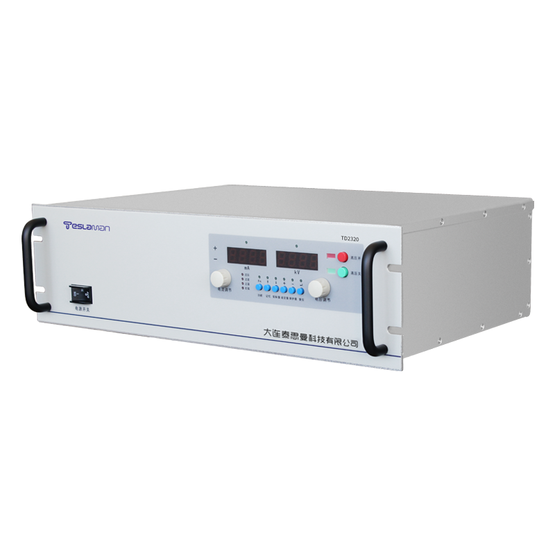
Ion Implantation Ultra-Shallow Junction Formation High-Voltage Power Supply
The relentless scaling of semiconductor devices has driven the need for ultra-shallow junctions (USJ) in source/drain extensions, with junction depths now required to be below 10 nanometers. Ion implantation remains a key technique for introducing dopants, but forming such shallow profiles requires extremely low implant energies, often below 1 keV, and sometimes in the range of 200-500 eV. Delivering a usable, stable ion beam at these energies presents extraordinary challenges for the high-voltage power supply responsible for accelerating (or, more accurately, decelerating) the ions. This supply operates in a unique regime where traditional high-voltage design principles are inverted, and stability is measured in single-electron-volt increments.
The primary challenge is beam transport. At energies of 500 eV or less, space charge forces—the mutual repulsion of positively charged ions in the beam—become dominant, causing the beam to blow apart and be lost before reaching the wafer. To mitigate this, the beam line is often designed to transport the ions at a higher, more stable energy (e.g., 5-10 keV) and then decelerate them just before the wafer. This places the final high-voltage power supply on the wafer stage or a dedicated deceleration electrode. The wafer is biased to a high positive potential (e.g., +9.5 kV) to decelerate a 10 keV positive ion beam down to 500 eV. Thus, the "high-voltage" supply is actually a positive, ultra-stable bias applied to the target, not to the ion source.
This deceleration supply must have phenomenal voltage stability and low noise. A variation of 1 volt at a 10 kV deceleration potential changes the final beam energy by 1 eV, which is a significant fraction of the total 500 eV energy. This directly affects the implant depth profile. Required stability is in the range of 0.5-1 V RMS, or 50-100 PPM. Achieving this at 10 kV is a severe test of reference stability, temperature control, and output stage design. The supply is almost invariably a linear regulator topology to achieve the necessary wideband noise performance. It uses an oven-controlled voltage reference, precision bulk-metal-foil resistor networks for feedback, and a series-pass tube or transistor array capable of handling the required current (up to tens of milliamps, as it must sink the entire implant beam current).
Furthermore, the load is not static. The beam current constitutes a current sink for this positive supply. As the ion beam is scanned across the wafer, the current draw is constant, but any instability in the beam current from the source will manifest as a load transient on the deceleration supply. Its feedback loop must have high bandwidth to reject these load-induced voltage fluctuations. Additionally, the supply must be immune to disturbances from other high-voltage systems in the end station and from RF generators used for plasma flood systems that neutralize wafer charging.
An alternative architecture for ultra-low-energy implantation is the "drift" mode, where the entire beam line, including the ion source, is floated at a high negative potential. The wafer is at ground. In this configuration, a massive negative high-voltage supply (e.g., -10 kV) powers the entire source and beam line assembly. The challenge here is insulating and powering all other subsystems—vacuum pumps, diagnostics, control electronics—that are attached to this floating high-voltage platform. This requires isolated power feeds and fiber-optic data links. The high-voltage supply itself must be extremely reliable, as a fault brings down the entire beam line. Its ripple and noise are equally critical, as they directly modulate the beam's final energy relative to the grounded wafer.
In both configurations, system integration and safety are extreme. All supplies involved have multiple, redundant arc detection and crowbar protection circuits. The transition from high-energy transport to low-energy implantation must be controlled to prevent energy contamination—the presence of a small fraction of ions that did not decelerate fully, creating an unwanted deeper implant tail. This often involves sophisticated electrostatic and magnetic filtering in the final stage. The ultra-shallow junction high-voltage power supply, through its unparalleled stability at the kilovolt level, enables the precise placement of dopant atoms within the first few atomic layers of silicon, a foundational capability for the continued miniaturization of transistors.