Reactive Ion Etching Load Effect Compensation Power Supply
Reactive Ion Etching (RIE) is a fundamental plasma etching process in semiconductor fabrication, prized for its anisotropic etching capability. A persistent challenge in RIE, particularly in batch processing or when etching patterned wafers with varying open area, is the "load effect." This refers to changes in etch rate, uniformity, and selectivity caused by variations in the total quantity of material being etched. The primary electrical manifestation of the load effect is a change in the plasma impedance, which in turn affects the coupling of radio frequency (RF) power into the plasma. The RF power supply, coupled with its impedance matching network, is the key subsystem that can be actively managed to compensate for these load-induced variations, moving from a passive power delivery role to an active process stabilization role.
The load effect arises because the reactive gases (e.g., CF4 for silicon etching, Cl2 for aluminum) are consumed in the etching reaction. A wafer with a large exposed area of material to be etched will consume more reactive species than one with a small area, lowering the concentration of etchants in the plasma. Concurrently, the reaction products (e.g., SiF4) are released, altering plasma chemistry. Electrically, this changes the plasma's density, electron temperature, and most notably for the RF system, its complex impedance. The impedance seen by the RF generator through the matching network shifts as the load changes. If the RF power is held constant in a traditional setpoint mode, the actual power *dissipated in the plasma* can change, leading to a shift in ion energy and flux, which directly impacts etch rate and anisotropy.
The first line of compensation is the automatic impedance matching network (matchbox). Its role is to maximize power transfer by tuning variable capacitors to cancel out the reactive component of the load and transform the resistive component to 50 ohms. While a fast matchbox can track slow impedance changes, it is a reactive compensator, not a proactive process controller. True load effect compensation requires a strategy that adjusts the RF generator's output parameters based on process feedback.
The most direct method is to switch from constant forward power mode to constant plasma parameter mode. This requires a sensor that provides a real-time signal correlated with the etching state. Two common sensors are used: a DC bias sensor and a plasma emission monitor (OES). The DC self-bias voltage (V_dc) that develops on the RF-driven electrode (the cathode) is a strong function of plasma density and ion energy. As the load changes, V_dc will shift if forward power is constant. Therefore, one compensation strategy is for the RF power supply to operate in constant V_dc mode. The generator's controller uses a feedback loop: it measures the actual V_dc (via a high-voltage probe and filter), compares it to a setpoint, and adjusts the generator's output power to maintain constant V_dc. This helps stabilize the ion energy, a key factor in etch anisotropy and selectivity, despite load variations. Implementing this requires an RF generator with an external analog or digital feedback input and a control loop with appropriate gain and stability margins.
Optical Emission Spectroscopy (OES) provides a chemical-specific signal. An emission line from a key reactant (e.g., F* at 704 nm) or product (e.g., SiF* or CO*) is monitored. A drop in reactant line intensity or a rise in product line intensity indicates increased loading. The RF power supply can be slaved to this signal, increasing forward power to increase dissociation and replenish the reactant concentration as more material is etched, thereby attempting to maintain a constant plasma chemical environment. This is a form of endpoint detection adapted for real-time control.
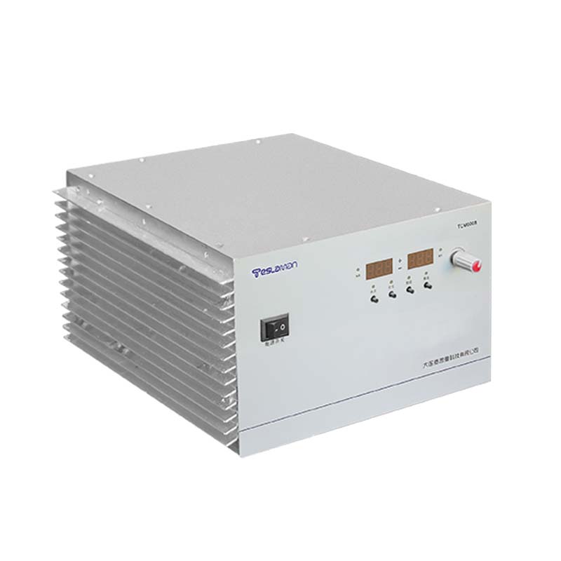
The RF power supply itself must be capable of this dynamic operation. It needs a fast control loop to adjust its output power smoothly and without oscillation in response to the feedback signal. The bandwidth of this loop must be sufficient to compensate for the time constants of the etching process and gas transport. Furthermore, the generator must be able to operate efficiently across a range of output powers and load impedances. Advanced generators use solid-state amplifier technology which offers wider operational bandwidth and faster response times compared to traditional tube-based amplifiers, facilitating more agile compensation strategies.
Integration with the matchbox is critical. In a constant V_dc control loop, the matchbox is continuously tuning to maintain impedance match as the generator changes its power. The control systems must be coordinated to avoid "fighting" each other. Some advanced systems integrate the generator and matchbox under a single digital controller, allowing for coordinated algorithms that adjust both power and matching simultaneously for optimal stabilization.
In summary, the RF power supply in a load-effect-compensated RIE system transitions from a simple energy source to the primary actuator in a real-time process control loop. By utilizing feedback from plasma electrical (V_dc) or optical (OES) parameters, it dynamically modulates RF power to counteract the changes in plasma state induced by varying etch load. This active compensation enhances process repeatability from wafer-to-wafer and within a wafer, improves etch uniformity across patterns with different feature densities, and is a critical enabling technology for achieving consistent results in advanced semiconductor manufacturing where device dimensions demand atomic-level precision.
