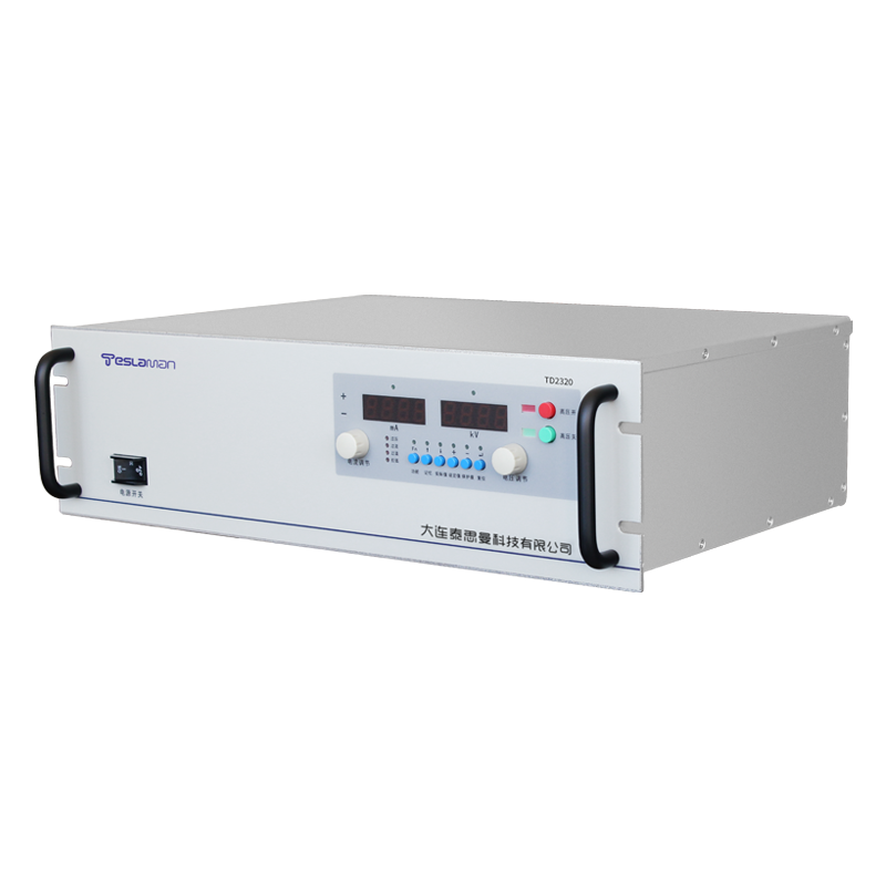
High-Voltage Power Supply for Electrostatic Chuck Edge Effect Compensation
In advanced semiconductor fabrication processes, particularly in plasma-enhanced etching and chemical vapor deposition, electrostatic chucks (ESCs) are indispensable for securing and thermally managing wafers. A persistent challenge in ESC operation is the edge effect, where the electrostatic clamping force exhibits non-uniformity near the wafer periphery. This non-uniformity can lead to localized thermal gradients, process non-uniformity, and wafer warpage, ultimately impacting yield. This article explores the specialized requirements for high-voltage power supplies designed to actively compensate for these edge effects, moving beyond simple bipolar or monopolar DC clamping. The fundamental cause of the edge effect lies in the fringing fields at the wafer's edge and the geometric discontinuity between the wafer and the chuck electrode pattern. Traditional ESCs apply a uniform DC voltage (often ±1-3 kV) to one or more electrode zones. However, this approach cannot dynamically adjust to the varying conditions that exacerbate edge non-uniformity, such as changes in wafer bow, backside gas pressure, or plasma sheath dynamics. An advanced compensation strategy involves the use of a multi-zone, independently controllable high-voltage power supply system. Here, the chuck contains a central electrode and one or more concentric ring electrodes. The power supply must provide isolated, stable, and rapidly adjustable high-voltage outputs to each zone. The core of compensation lies in real-time feedback control. Sensors monitoring parameters like wafer temperature (via embedded sensors) or clamp force inference models feed data to a controller. This controller then dynamically adjusts the voltage applied to the peripheral electrode zone relative to the central zone. For instance, to increase clamping force at the edge, the voltage differential between the edge electrode and the wafer is increased. This requires a power supply capable of precise voltage setpoint adjustments (often with millivolt resolution on the control signal) and excellent output stability with minimal ripple, as even minor voltage fluctuations can modulate the clamping force and induce vibration or thermal instability. Furthermore, the power supply must handle the unique load characteristics of an ESC, which is essentially a complex capacitor with a resistive component that can vary with temperature and surface contamination. The supply's output stage must be designed to source and sink current reliably, especially during the de-chucking phase, which often involves an active voltage reversal or an AC waveform to neutralize charge. For edge effect compensation, the transient response of the power supply is critical. The ability to slew voltages on the peripheral zones within tens to hundreds of milliseconds in response to a process step transition (e.g., moving from etch to deposition) is necessary to maintain consistent clamping throughout a recipe. This dynamic control effectively shapes the electrostatic field, creating a more uniform pressure distribution across the wafer's backside. This not only improves thermal contact for superior temperature uniformity but also minimizes microscopic wafer slippage, which is a known source of defects. Implementing such a system places stringent demands on the power supply's architecture: high-voltage isolation between channels to prevent cross-talk, low-noise design to avoid interfering with sensitive plasma diagnostics, and robust communication interfaces (like EtherCAT or proprietary digital links) for seamless integration into the equipment's main process controller. The result is a significant enhancement in process uniformity, enabling tighter critical dimension control at the wafer edge—a region that traditionally suffers yield loss—and facilitating the use of thinner, larger-diameter wafers where clamping uniformity is even more paramount.