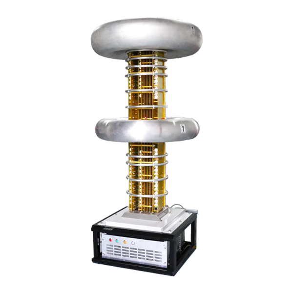
Ion Implantation Ultra-Low Energy High-Voltage Deceleration Power Supply
In advanced semiconductor manufacturing processes, ion implantation serves as a critical technique for introducing dopants into silicon substrates with extreme precision. The efficacy of this technique, especially at ultra-low ion energies below a few keV, is heavily dependent on the performance of the high-voltage deceleration power supply. This component is not merely a source of voltage; it functions as the central nervous system controlling the final kinetic energy of the ion beam before it impacts the wafer surface. At such low energies, the traditional challenges of beam transport, space charge effects, and energy contamination are magnified. The deceleration power supply must deliver a highly stable, low-ripple, and precisely programmable high-voltage output, typically in the range of tens of kilovolts, to decelerate ions extracted at a higher potential. Any minor fluctuation or instability in this output can lead to significant deviations in implantation depth profiles, directly affecting the formation of ultra-shallow junctions essential for modern transistors.
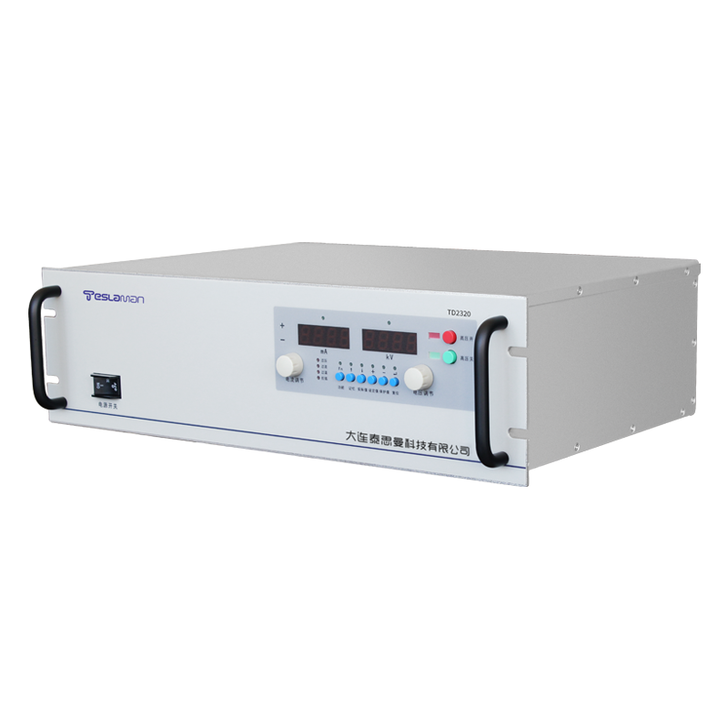
The architecture of such a power supply is inherently complex. It must incorporate advanced filtering and regulation topologies to achieve output ripple figures often specified in the single-digit millivolt range. This is paramount because even nanosecond-scale voltage transients can cause energy spreading, degrading the abruptness of the dopant profile. Furthermore, the supply must exhibit exceptional dynamic response. During beam tuning or at the start and end of an implant recipe, the voltage may need to change rapidly and settle to a new setpoint with minimal overshoot. This requires sophisticated digital control loops and high-frequency switching or linear regulation stages, all while maintaining complete isolation from ground-referenced control systems.
Another crucial aspect is the management of stored energy and arc handling. The high-voltage section stores considerable energy, and any internal breakdown or external arc event at the implanter's beamline or end station must be managed safely. The power supply must incorporate fast-acting arc detection circuits that can quench the output within microseconds, limiting the energy discharged into the plasma and protecting both the wafer and the implanter's internal components. Following an arc, the system must recover smoothly and re-establish the set voltage without introducing disruptive transients. This robust protection mechanism is non-negotiable for maintaining high wafer yield and tool uptime. In essence, the ultra-low energy high-voltage deceleration power supply is a pivotal technology enabler, pushing the boundaries of dimensional scaling in integrated circuits by allowing for precisely controlled, nanometer-scale doping layers.