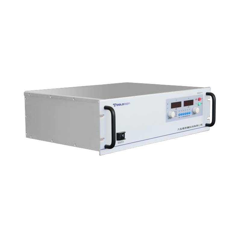
Electron Beam Multi-material 3D Printing High-Voltage Switching
Electron beam additive manufacturing, particularly for multi-material constructs, represents a frontier in advanced fabrication. The core of its capability to sequentially deposit disparate materials lies in the precision high-voltage switching system governing the electron beam source. Unlike conventional single-material electron beam melting, multi-material printing necessitates rapid, low-arcing transitions of the accelerating voltage, often in the range of 30 kV to 60 kV, to modulate beam energy and penetration depth instantaneously. This modulation directly influences the melt pool characteristics for each material, which possess varying thermal conductivity, latent heat, and electron scattering coefficients.
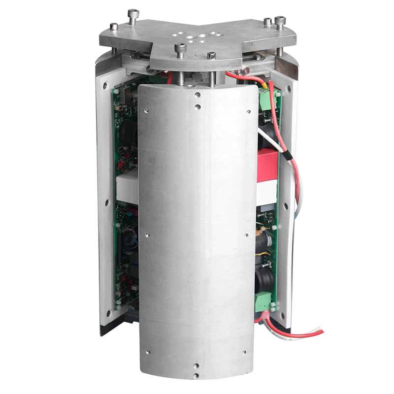
The high-voltage power supply for this application transcends the role of a simple energy source; it functions as a dynamic, fast-responding actuator. Key performance parameters include switching slew rates exceeding hundreds of volts per microsecond and settling times to within 0.1% of the target voltage in sub-millisecond durations. Any overshoot or ringing during the transition can induce defects such as interlayer porosity or unintended intermixing of materials at their interfaces. The power supply must therefore incorporate advanced closed-loop feedback mechanisms, utilizing precision resistive dividers and fiber-optic isolated voltage monitors to provide real-time data to the digital controller.
Electrical noise and electromagnetic interference (EMI) are paramount concerns. The rapid dv/dt generated during switching can couple into sensitive beam deflection and focusing coils, leading to beam spot instability. Mitigation strategies involve a multi-faceted approach: employing resonant or soft-switching topologies within the high-voltage generation circuitry to reduce harmonic content, implementing comprehensive shielding with mu-metal for critical components, and using star-point grounding schemes to prevent ground loops. The physical layout of high-voltage cabling, often utilizing coaxial designs with grounded outer sheaths, is critical to minimize parasitic capacitance that can distort the switching edge.
Furthermore, the power supply system must be intricately synchronized with the powder delivery mechanisms and the beam deflection system. A delay of even a few microseconds between voltage stabilization and material feeder actuation can compromise the dimensional accuracy of the material transition zone. This synchronization is typically managed via a centralized real-time controller issuing triggers over isolated communication protocols, ensuring the high-voltage state, beam position, and material feedstock are in perfect concordance. Reliability under continuous cyclical loading is non-negotiable, as industrial printing jobs may run for dozens of hours, demanding that the high-voltage switches and insulation endure tens of thousands of transitions without performance degradation. This necessitates rigorous derating of components and predictive maintenance scheduling based on thermal and electrical stress models.
The integration of such a power system also demands sophisticated software algorithms for voltage profiling. Rather than simple step changes, optimized transition waveforms—possibly featuring slight ramps or tailored shapes—can be programmed to manage thermal stress in the printed part more effectively. This level of control enables the fabrication of functionally graded materials with property gradients tailored for specific mechanical or thermal performance, unlocking new potentials in aerospace, medical implant, and energy storage device manufacturing.