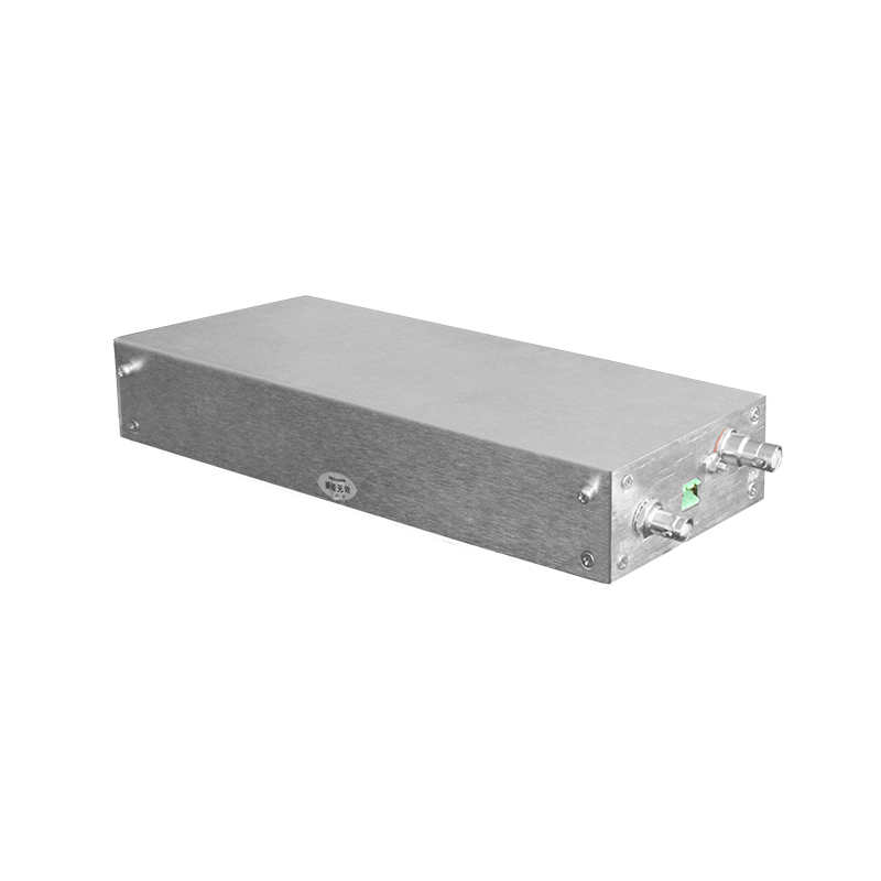
Proximity Effect Model Correction Power Source for Electron Beam Lithography
Electron beam lithography (EBL) is the workhorse for manufacturing photomasks and prototyping nanoscale devices. A fundamental resolution-limiting phenomenon in EBL is the proximity effect: the unintended exposure of resist in regions adjacent to the intended pattern due to electron scattering within the resist and substrate. While software-based model correction is standard, emerging hardware-based correction methods involve dynamic modulation of the beam itself during writing, placing unique demands on the high-voltage power supplies governing beam acceleration and blanking.
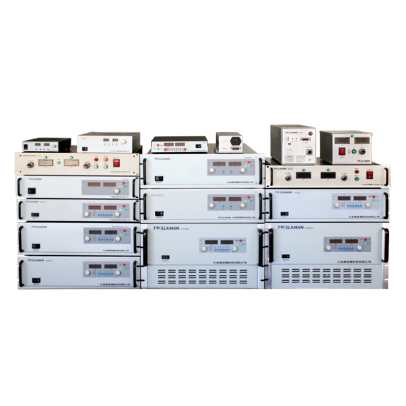
The traditional approach to proximity effect correction (PEC) relies entirely on post-processing of the design data, adjusting exposure doses per pixel. Hardware-assisted correction introduces a real-time, analog dimension by slightly modulating the landing energy of the electrons. Since electron scattering range is a function of incident energy, a small, fast variation in the accelerating voltage can change the shape of the exposure point spread function. A dedicated, ultra-stable, high-speed modulation power supply is connected in series with the main high-voltage column supply, adding or subtracting a precisely controlled offset voltage, typically in the range of tens to a few hundred volts, onto the base acceleration potential of 10 kV to 100 kV.
The performance requirements for this modulation supply are extreme. Its output noise and drift must be a minute fraction of the modulation amplitude, as any unintended voltage fluctuation directly translates into line edge roughness. Bandwidth is critical; to effectively correct for varying pattern densities across the writing field, the modulation must be capable of switching at rates commensurate with the beam blanking frequency, which can be in the megahertz range for shaped-beam systems. This demands a supply with a settling time to within 0.01% of the target offset in nanoseconds. Such performance rules out traditional linear amplifiers due to power dissipation and necessitates advanced switch-mode or linear-assisted switching topologies with exceptional feedback loop design.
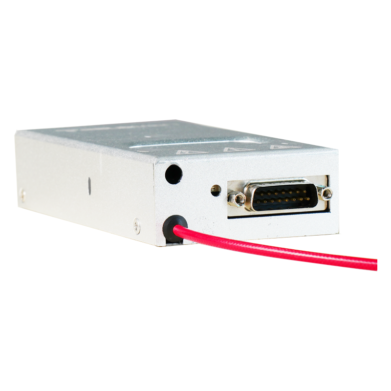
Integration into the existing electron optical column is a significant challenge. The modulation voltage must be injected at a point of high potential, requiring impeccable isolation and minimal added parasitic capacitance. Any stray capacitance at the injection node forms a low-pass filter with the column's internal resistance, potentially limiting the modulation bandwidth. Solutions often involve placing the compact modulation supply physically within the high-voltage tank of the main accelerator, using fiber-optic links for control and monitoring to maintain isolation. The supply must also be perfectly synchronized with the pattern data stream and beam deflection signals. A timing jitter between the voltage modulation and the beam's position on the substrate would create spatial errors worse than the proximity effect it aims to correct.
An alternative hardware PEC approach involves dynamic beam shaping through the blanking system. In this method, the intensity or profile of the beam spot is modulated at high speed. This requires the blanking amplifier, a high-voltage supply driving the electrostatic plates that deflect the beam off-axis, to possess not just fast switching but also precise analog control over its output voltage. The blanking waveform becomes a complex, non-binary signal that tailors the time-averaged exposure dose per pixel. The amplifier must have excellent linearity and low distortion to accurately reproduce these calculated waveforms. Furthermore, interactions between the modulated blanking signal and the beam deflection signals can occur through mutual capacitance or power supply coupling, requiring careful modeling and rejection in the amplifier design.
The ultimate benefit of integrating a model-correcting power source is the decoupling of resolution from total dose. By dynamically optimizing the energy or intensity per nanometer of travel, the exposure can compensate for backscattered electrons from neighboring features in real-time. This allows for the use of higher beam currents to increase throughput without sacrificing linewidth control, or enables the patterning of denser features with acceptable critical dimension uniformity. The power supply thus transitions from a static biasing component to an active, computational element of the lithography process, directly embedding the physical model of electron-matter interaction into the exposure tool's hardware execution loop.
