High-Voltage Adaptation for Ultra-Low Temperature Wafer Cooling in Ion Implantation
Ion implantation processes for advanced semiconductor nodes, particularly those involving high-dose, high-current species like boron or phosphorus, generate substantial thermal energy on the wafer. Uncontrolled wafer temperature leads to dopant diffusion, crystal damage annealing, and photoresist degradation, all of which compromise junction depth and profile accuracy. Actively cooling wafers to ultra-low temperatures, often in the range of -30°C to -60°C, during implantation has become a critical technique to freeze these thermal effects. However, integrating such cooling systems with the high-voltage electrostatics of the ion implanter presents a unique set of adaptation challenges.
The cooling is typically achieved by clamping the wafer to an electrostatic chuck (ESC) whose base is thermally linked to a cryogenic chiller via a coolant fluid. At these temperatures, the physical properties of materials change drastically. The most significant issue is the dramatic reduction in the electrical resistivity of the semiconductor wafer itself. Silicon, for instance, can see its resistivity increase by orders of magnitude as temperature drops, fundamentally altering its behavior as the counter-electrode in the ESC clamping circuit. At room temperature, a wafer has sufficient conductivity to quickly equalize surface potential. At -50°C, it behaves more like a semi-insulator, leading to non-uniform charge distribution, unstable clamping forces, and potentially dangerous charge buildup.
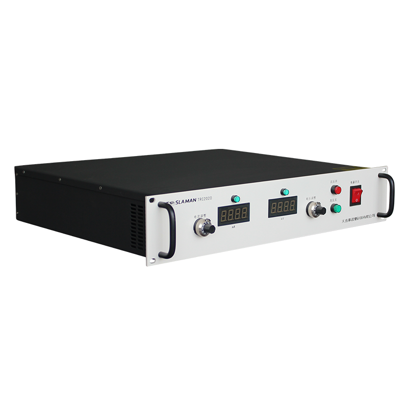
The high-voltage power supply for the cryogenic ESC must be specifically adapted to this high-resistivity regime. Standard Coulombic-force ESCs, which rely on an insulating layer between the electrode and wafer, become problematic as charge transport across this interface slows. This favors the use of Johnsen-Rahbek (JR) type clamping, which utilizes a slightly conductive dielectric to allow a small controlled current, ensuring charge replenishment at the wafer interface. The power supply must then be designed as a precision current-limited source rather than a purely voltage-limited one. It must regulate the microampere-level leakage current through the chuck to maintain a stable clamping force, even as the wafer's backside contact resistance and the chuck dielectric's conductivity vary with temperature.
Thermal gradients across the wafer during cooling can also induce triboelectric charging or pyroelectric effects in certain films, generating unpredictable localized voltages. The ESC power supply system must be robust against these transient potentials superimposed on its output. Furthermore, the act of applying a high voltage to a deeply cooled chuck carries a risk of condensing atmospheric moisture, leading to current leakage paths or arcing. Therefore, the entire ESC assembly and its high-voltage feedthroughs are housed in a high-vacuum environment, but the power supply design must still account for the possibility of outgassing from cold surfaces creating a transient local pressure rise.
Another critical adaptation involves the wafer bias supply. Some implantation schemes use a separate DC or RF bias on the wafer platen to control implant angle or energy. At ultra-low temperatures, the electrical connection to the wafer, often relying on the ESC's clamping force and the wafer's own conductivity, becomes highly resistive. This can lead to a significant voltage drop across the wafer, causing non-uniform implant energy across its diameter. The bias supply must either be capable of delivering higher currents to overcome this series resistance or, more effectively, the system design must incorporate a direct electrical contact mechanism, such as a set of sharp grounding pins, that pierces any native oxide on the wafer's backside. The bias supply must then be compatible with this pulsed or constant-contact loading.
Finally, system safety and control integration are paramount. The power supply must include dedicated sensors to monitor for condensation-induced leakage currents and have fast-acting protection to disconnect in case of an arc, which could vaporize coolant and cause a vacuum incident. Its control interface must be fully integrated with the cryogenic chiller's controller, allowing for coordinated ramp-down sequences where the chuck voltage is adjusted in sync with the wafer temperature to maintain constant clamping force. This closed-loop thermal-electrical co-optimization ensures that the wafer remains mechanically stable, electrically stable, and at a precisely controlled low temperature throughout the high-current implant cycle, enabling the formation of ultra-shallow, abrupt junctions required for cutting-edge transistors.