Synergistic High-Voltage for Ion Implantation Impurity Activation Annealing
Ion implantation, a cornerstone of semiconductor doping, introduces dopant atoms into a silicon lattice but leaves the crystal damaged and the dopants in interstitial positions, electrically inactive. Subsequent thermal annealing repairs the damage and activates the dopants by moving them into substitutional sites. Traditionally, these are separate steps: implantation using a high-energy ion beam followed by furnace or rapid thermal processing (RTP). The emerging concept of synergistic high-voltage processing seeks to merge or intimately couple these steps by applying tailored high electric fields during or immediately after implantation, aiming to enhance activation efficiency, reduce thermal budgets, and suppress undesirable dopant diffusion.
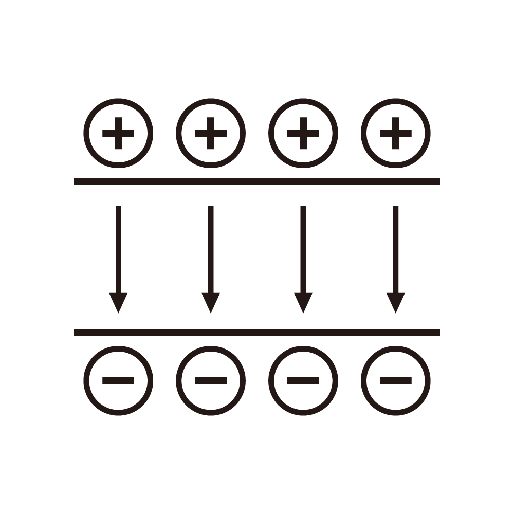
One approach involves the use of a high-voltage bias applied to the substrate during implantation itself. This is not the standard wafer bias used for energy adjustment, but a carefully controlled DC or pulsed potential that influences the initial damage cascade. When an ion strikes the lattice, it creates a trail of vacancies and interstitials. Applying a strong electric field across the wafer during this event can, in theory, influence the migration and recombination of these point defects. For instance, an electric field could promote the drift of charged vacancies away from the implant region, reducing the point defect density available for forming stable dislocation loops. Alternatively, it could affect the ionization state of the incoming dopant ions, altering their final stopping distribution. This requires a high-voltage supply integrated into the implant chamber, capable of operating in the presence of the beam and the high vacuum, with voltage levels that do not interfere with the beam optics but are sufficient to create fields of several kV/cm across the wafer thickness.
A more direct synergy occurs in post-implantation, in-situ annealing schemes. Here, the wafer remains within a modified process chamber after implantation. Instead of using only radiative heating, a high-current, low-voltage electron beam or a pulsed plasma is used to rapidly heat the wafer surface. The power source for this heating element, while often medium-voltage, must be coordinated with a separate high-voltage system that applies a bias across the wafer during the heating phase. This concurrent application of heat and electric field is the key. The field is believed to provide a directional driving force for charged dopant atoms (e.g., As+, B+) as they become mobile during annealing. This can potentially steer them toward substitutional sites more efficiently or counteract their tendency to diffuse laterally or cluster. The high-voltage supply for this purpose must be highly stable and noise-free, as any fluctuation in the field during the critical seconds of dopant mobility would introduce non-uniformities. It must also be designed to handle the changing electrical conductivity of the silicon wafer as its temperature rises from room temperature to over 1000°C in seconds, a dynamic load that presents a significant regulation challenge.
Another sophisticated method employs microwave-assisted annealing with a high-voltage DC bias. Microwaves couple energy directly to the silicon lattice and the dopant atoms, enabling very rapid and volumetric heating. When combined with a simultaneous DC field applied via electrodes on the wafer surface, the activation mechanism may shift. Research suggests that the microwave field can excite specific vibrational or rotational modes in defect complexes, while the DC field provides the directional force to break them apart or guide the dopant into place. The high-voltage DC supply in this configuration must be exceptionally well shielded to prevent any coupling or arcing with the high-power microwave field, which operates at GHz frequencies. This necessitates custom filtering and grounding schemes, often involving resonant cavities and waveguide-based isolation.
The practical implementation of these synergistic systems demands a holistic co-design of the high-voltage power supplies, the wafer chuck, and the process chamber. The chuck must provide reliable electrical contact to the wafer at high temperatures, which may involve novel backside metallization schemes or clamping forces. The power supplies must offer programmable sequencing: first, the implantation bias waveform, then a seamless transition to the annealing bias profile, all synchronized with the heating source's power ramp. Diagnostics are crucial; the system must include in-situ metrology like spectroscopic ellipsometry or resistance probes to monitor the activation process in real-time and provide feedback for the high-voltage parameters.
Ultimately, the goal is to achieve higher electrical activation with less thermal exposure, enabling the formation of ultra-shallow junctions for advanced transistor nodes and reducing the thermal budget that can degrade pre-existing device structures. The high-voltage system thus evolves from a mere biasing tool into an active participant in the solid-state physics of defect engineering, requiring a deep understanding of both electrical engineering and materials science to harness this synergy effectively.
