Synchronized High-Voltage Power Supply for Ion Implantation and Rapid Thermal Annealing
The ion implantation process introduces dopant atoms and lattice damage into silicon. Subsequent rapid thermal annealing (RTA) is used to repair the damage and activate dopants. Conventionally, these are separate tools with a wafer transfer in between. The concept of a synchronized high-voltage power supply refers to a system that performs implantation and initiates the annealing sequence within the same chamber, or in intimately linked chambers, with the high-voltage parameters of both stages co-optimized and sequenced by a single control system. This aims to exploit transient defect states and reduce total thermal budget for advanced junction formation.
In this synchronized scheme, the wafer resides on a platen that serves both as the target for the ion beam and as the heated stage for annealing. After the implant dose is complete, the ion beam is shut off, and the annealing cycle begins without breaking vacuum. The synchronization occurs on multiple levels. First, the high-voltage supplies for the implant beam must ramp down in a controlled manner. The extraction and acceleration high-voltage supplies (often totaling hundreds of kilovolts) are programmed to reduce their outputs smoothly to zero, minimizing voltage transients that could cause arcing or induce unwanted currents in the wafer. Simultaneously, the power supply for the wafer platen heater, which may be a medium-voltage, high-current source for lamp-based heating or a low-voltage, very high-current source for direct resistive heating, begins its ramp-up sequence.
The most critical aspect of synchronization is the management of the wafer potential. During implantation, the wafer is typically held at a specific bias potential, which may be ground, a small positive voltage to suppress secondary electrons, or a higher voltage for deceleration. During annealing, especially with lamp-based RTA, the wafer should ideally be electrically floating or grounded to prevent charging. The synchronized control system must manage the transition of the wafer chuck from a biased implant mode to a grounded/floating anneal mode. This is achieved using a high-voltage switch or relay connected to the wafer chuck bias supply. The timing of this switch opening must be precise, occurring after the beam is fully off but before significant heating begins, to prevent any discharge through the wafer that could damage sensitive devices.
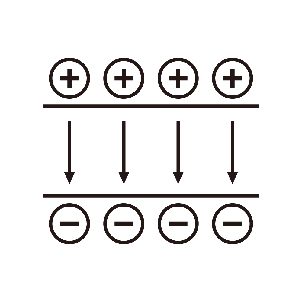
An advanced version of this concept applies an active bias to the wafer during the initial phase of annealing. The theory is that as the wafer heats rapidly, point defects and dopant atoms become mobile. Applying an electric field across the wafer during this critical phase could influence their migration. For example, a field could help sweep interstitial silicon atoms away from the doped region, reducing transient enhanced diffusion (TED) of boron. Or, it could provide a directional force to guide charged dopants into substitutional lattice sites. This requires a dedicated, stable high-voltage supply (in the 100V to 1kV range) that is activated precisely at the start of the thermal ramp. This supply must operate reliably while the platen temperature rises from ambient to over 1000°C in seconds, a significant challenge for insulation and contact reliability.
The integrated control system for such a tool is complex. It must sequence the implant high-voltage supplies, the wafer bias supply, the bias switch, and the anneal heater supply based on a single recipe. Safety interlocks are multiplied; for instance, the implant high voltage must be interlocked with a verified wafer temperature being below a threshold, and the annealing heater must be interlocked with a verified beam current of zero. Data logging must capture the complete time-history of all these voltages and currents alongside wafer temperature to provide a complete process trace.
The benefits target the most advanced nodes. By minimizing the time between implant and anneal, certain metastable defect complexes may be annealed out before they can evolve into more stable, detrimental defects. The reduced thermal budget from a faster, in-situ anneal limits dopant diffusion, enabling shallower, more abrupt junctions. The synchronized high-voltage system is the enabling orchestrator of this coupled physical process, treating implantation and annealing not as discrete steps but as a continuous, coordinated materials transformation event.
