Low Accelerating Voltage Power Supplies for Compositional Contrast in Scanning Electron Microscopy
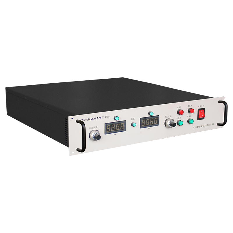
The scanning electron microscope is a cornerstone instrument for microstructural and nanoscale characterization. While high accelerating voltages are traditionally used for high-resolution imaging and X-ray microanalysis, there is a growing and critical need for operation at low accelerating voltages, typically below 5 kilovolts and often down to a few hundred volts. This low-voltage regime is essential for examining beam-sensitive materials, reducing charging on insulating specimens, and, most pertinently here, enhancing compositional or material contrast based on differences in secondary electron yield. The power supply that provides this low accelerating voltage is a specialized component whose performance dictates the quality and reliability of this imaging mode.
At low beam energies, the interaction volume of electrons with the sample becomes very shallow, often limited to just a few nanometers. This makes the signal highly surface-sensitive. The yield of low-energy secondary electrons, which is the primary signal for topographic and compositional contrast imaging, is strongly dependent on the work function and electronic structure of the material. Different phases or elements exhibit different secondary electron emission coefficients at a given beam energy. This natural contrast can be profoundly pronounced at carefully selected low voltages. However, to exploit this phenomenon, the electron beam must possess a stable, well-defined low energy, which is the direct responsibility of the high-voltage power supply.
Designing a high-voltage supply for stable operation at 1 kilovolt is, in many ways, more challenging than for 30 kilovolts. The primary issue is the ratio of unwanted noise or ripple to the total output voltage. A 100-millivolt ripple on a 30-kilovolt output represents 0.003% ripple, which is often acceptable. The same 100-millivolt ripple on a 1-kilovolt output is 0.1% ripple, and on a 500-volt output it becomes 0.2%. This ripple directly modulates the beam energy, causing the secondary electron yield to fluctuate during the pixel dwell time. The result is a degradation of signal-to-noise ratio and the introduction of fine striations or blur in the image. Therefore, low-voltage SEM supplies demand exceptionally low output noise, often specified in the single-digit millivolt range. Achieving this requires linear regulation stages, ultra-stable voltage references, and filtering components with extremely low parasitic inductance and capacitance.
Stability over time and temperature is equally critical. Drift in the output voltage, even at a rate of a few volts per minute, would cause the compositional contrast to change during a slow-scan image acquisition, making quantitative comparison across the image field invalid. The supply must be designed with low-drift components and a tightly controlled thermal environment. Often, critical circuits are housed in an oven-controlled enclosure to maintain a constant temperature, mitigating drift from ambient changes in the laboratory.
Another key feature is the precision of voltage selection. To find the optimum voltage for contrast between two specific phases, an operator may need to sweep the accelerating voltage in fine steps, perhaps as small as 10 or 20 volts, while observing the image. The power supply must offer this fine control resolution across its entire low-voltage range. This is typically achieved with high-resolution digital-to-analog converters in the control loop. The interface must allow for both manual fine adjustment and programmable voltage sweeps.
The transition between high and low voltage modes is also a consideration. Modern SEMs are versatile tools. A user might perform analysis at 15 kV and then switch to 1 kV for surface imaging. The high-voltage supply must be capable of this wide dynamic range operation. It must ramp voltages up and down in a controlled manner to avoid arcing within the column or causing large transient beam currents. Some designs incorporate separate regulation circuits optimized for different voltage bands, with seamless switching between them.
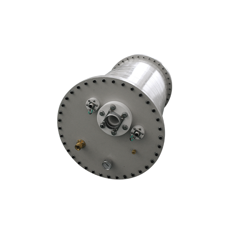
Furthermore, the interaction with the electron gun design is profound. At very low voltages, space charge effects can cause significant beam broadening, degrading resolution. Some systems employ a beam booster, where the cathode is held at a high negative potential (e.g., -5 kV), and the anode is at a slightly less negative potential (e.g., -4.9 kV) to create a 100-volt beam. This requires a multi-output supply with precisely tracked voltages. The stability and tracking accuracy between these outputs become paramount, as any difference directly defines the net beam energy.
In application, the benefits of a well-engineered low-voltage power supply are directly visible. It enables the clear differentiation of phases in multi-material systems—such as distinguishing carbon fibers from a polymer matrix, or observing grain boundary phases in ceramics—without the need for conductive coatings. It allows for the inspection of photoresist patterns, organic films, and biological samples with minimal damage. The power supply, in providing this stable, precise, and clean low voltage, becomes the enabler for a whole class of advanced materials characterization that relies on subtle electronic surface properties rather than merely atomic number contrast.