High-Voltage Assisted Fabrication of Colloidal Crystal Templates for Electron Beam Lithography
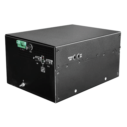
The creation of large-area, defect-free photonic crystals and patterned nanostructures often relies on high-resolution templates. Colloidal crystals, formed by the self-assembly of monodisperse nanospheres, provide a versatile and cost-effective templating method. However, achieving perfect long-range order and transferring these patterns into functional substrates via subsequent electron beam lithography or etching steps presents significant challenges. A promising approach to enhance this process involves the use of high-voltage fields during the colloidal assembly or subsequent processing stages. This high-voltage assistance is not for the e-beam itself, but for preparing an ideal template, and it requires a specialized power system designed for interaction with colloidal suspensions and delicate nanostructures.
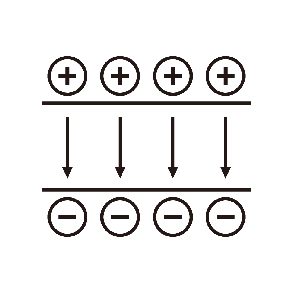
One primary application of high voltage is in the electrophoretic deposition of colloidal particles. Instead of relying solely on gravitational settling or convective assembly, an electric field can be applied across a cell containing the colloidal suspension. The charged particles migrate toward the electrode of opposite polarity, depositing onto a conductive substrate. A high-voltage DC power supply, typically in the range of tens to a few hundred volts, drives this process. The critical requirement here is not high voltage per se, but extreme stability and cleanliness. Any ripple or noise on the applied field causes fluctuations in the electrophoretic force, leading to variations in deposition rate and ultimately defects in the crystal lattice. The supply must provide a perfectly smooth DC potential, often requiring linear regulation and battery-like noise performance.
More sophisticated techniques involve using alternating current or shaped electric fields to guide the assembly. For instance, applying an AC field at a specific frequency can induce dipolar interactions between particles, encouraging them to align into crystalline domains more rapidly and with fewer defects than in passive assembly. This requires a high-voltage amplifier capable of generating stable sine waves from a few hertz to several megahertz, with voltages up to perhaps a kilovolt peak-to-peak. The amplifier must drive the capacitive load of the deposition cell without phase shift or harmonic distortion, as the assembly kinetics are sensitive to the exact field waveform. Programmable frequency and amplitude allow researchers to tune the assembly process for different particle sizes and materials.
After deposition, the colloidal crystal template may require stabilization or modification before being used as a mask for electron beam lithography. Here, high voltage finds another role in a process akin to nano-electrospinning or electrowetting. A very high voltage (several kilovolts) can be applied in a controlled manner to slightly sinter or fuse the points of contact between adjacent polymer spheres, strengthening the template without fully melting it and destroying the order. This demands a supply with precise current limiting, as the conduction through the nanoscale contacts is minute and unstable; a standard supply might easily over-current and cause a runaway thermal event.
Integration with the subsequent e-beam lithography step is a key consideration. The template, now on a substrate, is placed in the e-beam system. If the template or substrate retains any residual charge from the high-voltage assembly process, it can deflect the scanning electron beam, causing massive pattern placement errors. Therefore, the high-voltage systems used in template preparation must include robust discharge circuits and grounding protocols to ensure the final template is electrically neutral before entering the high-vacuum chamber. In some integrated setups, a final in-situ low-energy plasma treatment, powered by a separate high-frequency high-voltage source, might be used to gently remove any residual organics and neutralize surface charge immediately before e-beam exposure.
From a practical research and development standpoint, the high-voltage equipment for this application sits at the intersection of colloidal chemistry, soft matter physics, and nanofabrication engineering. It must be versatile, allowing for easy connection to custom deposition cells, and safe for use around liquids and conductive substrates. User interfaces that allow for programming complex voltage-time profiles (e.g., a ramp followed by an AC oscillation, then a DC hold) are essential for exploring new assembly paradigms.
Ultimately, the use of optimized high-voltage fields in colloidal crystal fabrication is a force multiplier. It accelerates assembly, improves domain size and reduces defects, and enables the creation of more complex template geometries, such as binary colloidal crystals or non-close-packed arrays. By providing a more perfect starting template, it dramatically improves the fidelity of the final nanostructures produced by electron beam lithography, leading to better-performing photonic devices, plasmonic sensors, and structured surfaces with tailored optical and wetting properties.
