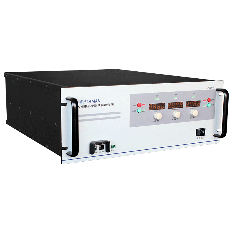
Plasma Modulation High-Voltage Source for Atomic Layer Etching
Atomic Layer Etching (ALE) is a next-generation semiconductor processing technique that removes material with ultimate precision, one atomic layer at a time, by separating the chemical modification and physical desorption steps. Plasma-based ALE often uses alternating exposure of the wafer to a reactive gas (e.g., a halogen) and an energetic ion flux (typically argon). The control of the ion energy and flux during the desorption step is critical to achieving true layer-by-layer removal without damaging the underlying material. This control is achieved through a plasma modulation high-voltage source that applies tailored, pulsed bias to the wafer substrate.
In a typical ALE cycle, the wafer is first exposed to a reactive gas plasma, which forms a thin, self-limiting modified layer on the surface. The chamber is then purged. Next, an argon plasma is ignited, and a pulsed bias is applied to the wafer to attract ions. The ions bombard the modified layer, providing the energy to break its bonds and desorb the reaction products, ideally removing exactly one monolayer. The key is that the ion energy must be high enough to desorb the modified layer but low enough to not sputter or damage the pristine material beneath it—a window often only a few tens of electron volts wide.
The high-voltage source providing this pulsed bias must meet extraordinary specifications. First, it must produce very stable, low-noise pulses in a precisely controlled energy range, typically from 20 eV to 200 eV. Since ion energy is roughly equivalent to the applied bias voltage (minus a plasma sheath potential), this translates to pulse amplitudes from tens to a few hundred volts. However, the stability requirement is extreme; a 5-volt drift can represent a 25% change in ion energy, potentially moving out of the process window. The pulse shape is also critical. A square wave with fast rise and fall times is desired to create a clear temporal separation between the modification and etch steps and to ensure all ions within a pulse have nearly identical energy.
Second, the source must operate at a frequency compatible with the ALE cycle time. Cycle times can range from a few seconds to sub-seconds, requiring pulse repetition rates from below 1 Hz to several hertz. The source must be synchronized perfectly with the gas injection and plasma ignition sequences from the main tool controller. Third, and most challenging, the source must drive a highly non-linear and dynamic load—the plasma sheath. When the bias pulse is applied, the plasma sheath forms and collapses with each pulse. The source must be able to source and sink current rapidly to maintain the set voltage during this dynamic transition. This requires a power supply with high bandwidth and low output impedance.
Advanced ALE processes use more complex waveforms than simple square pulses. To further narrow the ion energy distribution, a tailored pulse with a specific rise time or a multi-level pulse can be used. Some schemes employ a very short, high-voltage pulse to quickly form the sheath, followed by a longer, lower-voltage plateau for the actual etching. This demands a programmable, arbitrary waveform high-voltage amplifier. Furthermore, the source often needs to be coupled to the wafer through a capacitive coupling network or a matching network to work effectively with the RF plasma used to generate the argon ions, adding another layer of complexity to the impedance matching.
The integration of this modulated bias source is what enables the self-limiting characteristic of ALE. By precisely controlling the ion energy dose per cycle, the process can be made highly selective and atomic-layer precise. This level of control is indispensable for etching the ultra-thin films and complex three-dimensional structures (like FinFETs and 3D NAND memory cells) of modern semiconductor devices, where even nanometer-scale non-uniformity or damage is catastrophic. The high-voltage source thus becomes the master regulator of the etch stop, translating digital process recipes into perfectly controlled atomic-scale removal.