High-Voltage Correction of Gain Uniformity in Microchannel Plate Detectors
Microchannel plate detectors are ubiquitous in scientific instrumentation, from night vision and photon counting to mass spectrometry and particle physics. They consist of an array of millions of microscopic glass capillaries, each acting as an independent continuous-dynode electron multiplier. When a charged particle or photon strikes the input face, it initiates an electron cascade within a channel, resulting in a detectable pulse of 10^4 to 10^7 electrons at the output. While conceptually simple, achieving uniform gain across the entire active area of a large-format MCP is a persistent challenge. Local variations in channel geometry, wall surface chemistry, and contamination inevitably cause gain non-uniformity, which appears as fixed-pattern noise in the final image. A powerful and elegant method to correct this non-uniformity is through the application of a spatially variable high-voltage bias across the plate, a technique that demands an exceptionally sophisticated high-voltage control system.
The gain of a microchannel plate is a steep, exponential function of the voltage applied across it, from the input to the output surface. A typical MCP might operate at 800 to 1200 volts, and a one percent change in voltage can result in a five to ten percent change in gain. This extreme sensitivity, while a challenge, also provides the mechanism for correction. If a region of the plate exhibits lower intrinsic gain, raising the local voltage across that region will increase its gain to match the higher-gain areas. Conversely, locally reducing the voltage can suppress an excessively hot spot. This is the principle of voltage-division correction or active gain trimming.
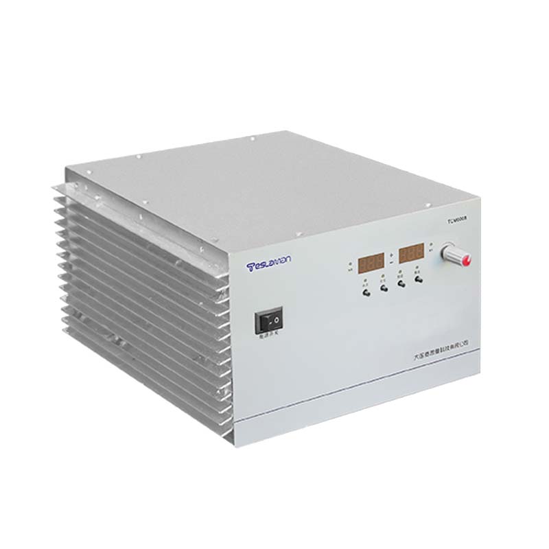
The implementation of this correction is not trivial. It cannot be achieved with a single uniform power supply. The solution involves segmenting the output electrode (or sometimes the input electrode) of the MCP into a mosaic of isolated conductive pads, each connected to an independent high-voltage bias supply. Alternatively, a resistive layer with a patterned current injection system can be used to create a continuous potential map. The power supply system must, therefore, provide tens or even hundreds of independently programmable high-voltage outputs, each capable of delivering a stable, low-noise voltage in the range of 0 to 1000 volts, with microampere current capability, and all referenced to a common cathode potential.
The first step in implementing such a system is characterization. The uncorrected gain uniformity of the MCP is measured by flooding it with a uniform illumination source and recording the output image. This calibration map is stored in the control system memory. The control system then executes a correction algorithm, which translates the desired gain correction factor for each pixel or zone into a required voltage adjustment. This translation must account for the nonlinear voltage-gain relationship of the specific MCP type and its current operational state, as gain also depends on total output current (gain saturation). The algorithm computes a target voltage for each zone and commands the respective high-voltage channel to that setpoint.
The demands on the high-voltage power supplies for this task are extreme. First, stability is non-negotiable. If the voltage on one correction zone drifts by only 0.1 volt relative to its neighbors, the gain difference will become visible as a contour in the flat-field image. Therefore, each channel must incorporate an ultra-stable voltage reference and a control loop with extremely low temperature drift. Second, resolution is critical. To achieve fine-grained correction, the supply must have high-resolution digital-to-analog conversion, often 16 bits or more, to allow for millivolt-level adjustment steps. Third, noise must be essentially zero. Ripple or random noise on a correction zone voltage will be multiplied by the MCP gain and appear as a temporal noise source in the region of the image served by that zone, degrading the signal-to-noise ratio of the measurement.
Another layer of complexity is the interaction between zones. The potential on one pad influences the fringe fields on its neighbors. The correction algorithm must therefore be iterative or incorporate a model of the electrostatic coupling to avoid creating a pattern of its own. In advanced systems, the controller periodically re-measures the flat-field response and fine-tunes the channel voltages in a closed-loop manner, ensuring the correction remains perfect as the MCP ages or the count rate changes.
In some high-speed or gated applications, the MCP voltage is pulsed to achieve nanosecond time resolution. The correction system must operate in this pulsed environment. This requires that the individual channel supplies either maintain their precise DC bias during the pulse, or that the pulsing waveform itself is programmable per zone. The latter is a monumental challenge, requiring an array of high-voltage pulsers with matched timing and independent amplitude control.
The physical packaging of such a system is also a major engineering endeavor. Hundreds of high-voltage cables must be brought into the vacuum chamber and connected to the back of the MCP stack without introducing mechanical stress on the fragile plate assembly or compromising the vacuum integrity. Specialized multi-pin feedthroughs with high voltage rating and ultra-high vacuum compatibility are essential.
Ultimately, a well-implemented high-voltage gain correction system transforms a mediocre MCP detector into a precision scientific instrument. It enables large-area photon-counting detectors with spatial uniformity that rivals solid-state sensors, making them ideal for applications such as space-based astronomy, high-energy physics experiments, and fluorescence lifetime imaging microscopy. The high-voltage system, in this context, becomes an active optical element, shaping the gain landscape of the detector to cancel out the imperfections of its physical fabrication. It is a prime example of using advanced electrical engineering to overcome the fundamental limitations of a mature technology.