High-Voltage Optimization for Low-Voltage Backscattered Electron Imaging in Scanning Electron Microscopy
Backscattered electron (BSE) imaging in a scanning electron microscope (SEM) provides compositional contrast, as the BSE yield is a monotonic function of the atomic number of the sample. Traditionally, BSE imaging is performed at relatively high beam accelerating voltages (10-30 kV) to ensure a strong signal. However, for many samples, particularly those that are beam-sensitive (e.g., polymers, biological tissue) or when surface sensitivity is paramount, low-voltage operation (1-5 kV) is highly desirable. At these low voltages, the BSE signal is much weaker, and the detector response is strongly influenced by the energy distribution of the returning electrons. Optimizing the high-voltage bias applied to the BSE detector itself is the key to unlocking high-quality compositional imaging at low beam energies.
The most common BSE detectors are scintillator-based, where a material (e.g., YAG or P47 phosphor) emits light when struck by high-energy electrons. This light is then guided to a photomultiplier tube (PMT). The efficiency of this process, particularly the light output of the scintillator, is strongly dependent on the energy of the incident electrons. At low beam voltages (e.g., 3 kV), the BSEs have very low energy. Many will not have enough energy to penetrate the detector's entrance window or to generate a detectable light pulse in the scintillator. The solution is to accelerate the BSEs before they hit the scintillator.
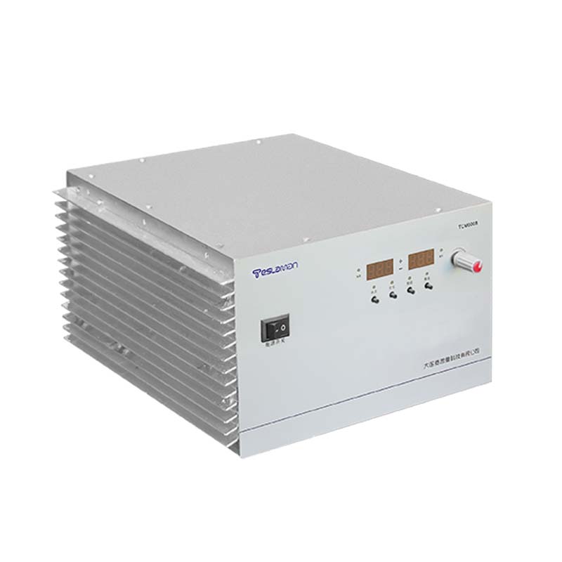
This is achieved by applying a high positive bias (typically +10 kV to +15 kV) to the scintillator itself, or to a grid in front of it. The BSEs, which are negatively charged, are strongly attracted and gain kinetic energy as they cross the potential difference. A 3 keV electron is now a 13 keV electron when it strikes the scintillator, producing a much brighter flash. The high-voltage supply for this scintillator bias must be extremely stable and low-noise. Any ripple on this bias modulates the final energy of the BSEs and thus the light output, introducing noise into the image.
However, the optimization does not stop at simply applying a high bias. The detector geometry and the bias voltage must be carefully tuned to ensure that the collection efficiency is uniform across the field of view and that it does not interfere with the primary beam or other detectors. The electric field from the biased scintillator can extend into the chamber, potentially deflecting the primary beam or distorting the image. Therefore, the detector is often housed within a shielded cage with a grid held at an intermediate potential, or it is designed with a very localized field.
Furthermore, the energy filtering capability can be exploited. By applying a bias that is only slightly above the primary beam energy, the detector can be made to selectively collect only the highest-energy BSEs, which originate from deeper within the sample and carry the strongest compositional signal, while rejecting the lower-energy secondary electrons and BSEs from the surface. This is a form of energy-selective imaging performed by the detector bias itself.
For advanced applications, the detector bias can be dynamically modulated during the scan. For instance, when scanning across a region with a large change in atomic number, the bias can be adjusted on a line-by-line basis to maintain a constant signal level in the detector, preventing saturation and optimizing the use of the ADC's dynamic range. This requires a fast, programmable high-voltage supply that can respond to a control signal from the SEM's scan generator.
The integration of this optimized high-voltage bias with the rest of the SEM's control system is seamless to the operator. The user selects the desired beam voltage and the desired imaging mode (e.g., compositional or topographic), and the system automatically sets the optimal detector bias. The result is high-resolution, high-contrast compositional imaging of delicate samples at beam energies low enough to avoid damage, opening up new possibilities in the study of soft materials, biological structures, and thin films. The high-voltage supply, once a simple accessory, becomes an integral part of the imaging optics, its precise voltage defining the very energy of the signal that forms the image.