High-Voltage Induced Self-Assembly of Colloids in Electron Beam Direct-Write Lithography
Electron beam lithography has long been the workhorse for generating the ultra-fine patterns needed in photomask fabrication and advanced device prototyping. Its resolution is unmatched, but its serial nature makes it slow for large-area patterning. To bridge this gap, researchers and engineers have been exploring hybrid approaches that combine the precision of electron beams with the parallel, self-organizing capabilities of colloidal materials. The concept is elegant: use an electron beam to write not every pixel of a final structure, but rather to define guiding templates or to create localized electric fields that direct the self-assembly of nanoparticles or block copolymers into desired patterns. In this emerging field, the high-voltage power supply of the electron microscope or lithography tool takes on a new and critical role. It is no longer just the source of the imaging or exposing beam; it becomes a tool for generating and controlling the electrostatic forces that drive the self-assembly process. After fifty years of working with electron beams, I am particularly fascinated by this development, as it represents a profound shift in how we think about beam-matter interactions.
The most direct method of high-voltage induced self-assembly involves using the electron beam to charge specific areas of a substrate. When an insulating or semiconducting substrate is exposed to an electron beam, a portion of the primary electrons become trapped, creating a localized region of negative charge. This charge generates a strong, non-uniform electric field that can extend tens of nanometers or even micrometers above the surface. If the substrate is then exposed to a dispersion of charged colloidal particles or nanoparticles, these particles will experience a dielectrophoretic or electrophoretic force that attracts them to the charged region. By carefully controlling the beam parameters, such as the accelerating voltage, the beam current, and the dwell time, we can control the amount of charge deposited and, consequently, the strength and extent of the trapping field. The particles will then self-assemble into patterns that mirror the written charge distribution. This technique, sometimes called charge-directed assembly, offers a way to create complex nanoparticle arrays without the need for a physical template.
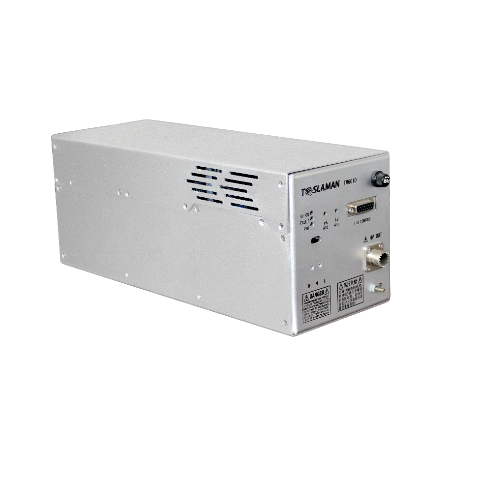
The high-voltage stability of the electron beam is absolutely critical in this process. The amount of charge deposited is a function of the beam current and the dwell time. Any fluctuation in the accelerating voltage will change the beam energy, which in turn affects the penetration depth and the secondary electron yield, altering the net charge deposited. A 1% ripple in the high voltage can lead to a significant variation in the surface potential, causing inconsistencies in the particle assembly. The power supply must therefore be exceptionally stable, with ripple and drift measured in parts per million. Furthermore, the beam must be able to be blanked and unblanked with extremely fast rise and fall times to create sharp charge patterns. The blanking system, often a pair of electrostatic deflectors driven by a high-voltage pulser, must be synchronized with the beam movement to ensure that charge is deposited only in the intended locations.
Beyond direct charging, a more sophisticated approach involves using the electron beam to modify the surface chemistry in conjunction with an applied external field. For example, the substrate might be coated with a thin layer of a photoresist or a self-assembled monolayer. The electron beam can be used to cross-link or to cleave chemical bonds in this layer, creating a pattern of chemically distinct regions. Subsequently, a high-voltage bias is applied between the substrate and a counter-electrode in the colloidal solution. This external field drives the electrophoretic motion of the particles, while the chemical pattern dictates where they will adhere. In this scenario, the high-voltage supply for the external bias must be independent of the microscope column supply. It must be capable of providing a stable, programmable voltage, often in the range of tens to hundreds of volts, and it must be carefully isolated from the sensitive electronics of the microscope to prevent ground loops and interference. The combination of electron beam writing and external field control offers a powerful and flexible platform for creating hierarchical structures with features spanning multiple length scales. In my view, this marriage of top-down electron beam lithography and bottom-up self-assembly, orchestrated by precision high-voltage systems, represents a major frontier in nanofabrication. It allows us to harness the inherent efficiency of self-organizing systems while retaining the ultimate control and pattern fidelity of a direct-write beam, opening the door to new classes of materials and devices that are impossible to create by either method alone.