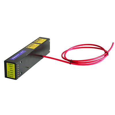
High-Voltage Period Modulation for Superlattice Thin Films in Magnetron Sputtering
Superlattice thin films, composed of alternating nanoscale layers of two different materials, exhibit remarkable properties that are not found in either constituent alone. These properties, which include giant magnetoresistance, enhanced hardness, and tailored optical responses, arise from the quantum confinement of electrons and the elastic interactions between the layers. The fabrication of these structures with the required precision, where individual layer thicknesses are controlled to within a single atomic monolayer, is a significant challenge. Magnetron sputtering, with its ability to produce smooth, dense films over large areas, has emerged as a leading technique for superlattice deposition. However, to achieve the necessary layer thickness control, the sputtering process must be modulated with extraordinary precision. This is where the high-voltage power supply takes on a critical role. By precisely modulating the voltage applied to the sputtering cathodes, we can control the deposition rate in real-time, creating the periodic structure required for a superlattice. In my five decades of work in thin film deposition, I have seen the evolution from simple DC sputtering to the sophisticated, pulsed and modulated techniques that enable the synthesis of these artificial materials with atomic-scale precision.
The conventional method for depositing a superlattice is to use two separate magnetron cathodes, each with a target of a different material, and to alternately expose the substrate to each source. This can be done by rotating the substrate on a carousel between the two sources, or by using shutters to alternately block and unblock the flux from each source. While effective, this mechanical approach is limited in speed and precision. The substrate movement or shutter actuation introduces dead time, and the deposition rates can drift over time, leading to errors in layer thickness. A more elegant and precise approach is to use a single, stationary substrate and to modulate the power delivered to each cathode. By rapidly switching the high voltage on and off, or by varying its amplitude, we can effectively turn the deposition from each source on and off electronically, with switching times that are orders of magnitude faster than any mechanical system. This is the essence of high-voltage period modulation for superlattice growth.
The implementation of this technique requires a high-voltage power supply with exceptional dynamic performance. For a simple on-off approach, the supply must be capable of being turned on and off very rapidly, with rise and fall times measured in microseconds or less, to create sharp interfaces between layers. If the voltage ramps up or down too slowly, a graded interface will be formed, blurring the superlattice structure. The supply must also be capable of operating at a high repetition rate, as the individual layers in a superlattice can be as thin as a few angstroms, requiring deposition times of only a few seconds or even fractions of a second. For a more advanced approach, the voltage can be modulated not just on and off, but between two or more precise levels. For example, to deposit a layer of material A, the voltage on cathode A is set to a high value, while cathode B is kept at a low, non-sputtering bias. To deposit material B, the voltages are swapped. This requires a multi-channel high-voltage system where each channel can be independently programmed and where the transitions between states are fast and well-controlled. The synchronization of the voltage modulation with any substrate motion or with the rotation of a carousel, if used, adds another layer of complexity. The control system must ensure that the voltage transitions occur precisely when the substrate is in the optimal position relative to each source.
The stability of the voltage during the on period is just as critical as the switching speed. Any ripple or drift in the voltage will translate into a variation in the sputtering rate, leading to layer thickness non-uniformity. For a superlattice with hundreds of layers, even a tiny error in each layer can accumulate, destroying the desired structure. Therefore, the high-voltage supply must have exceptional long-term stability, with drift measured in parts per million over hours of operation. It must also be immune to the effects of target erosion, which can change the impedance of the plasma over time. A feedback loop that monitors the plasma current or optical emission and adjusts the voltage to maintain a constant deposition rate is often employed. In my experience, the synthesis of high-quality superlattices is a true test of the limits of high-voltage engineering. It demands a power supply that is simultaneously fast, stable, and precise, capable of executing a complex modulation pattern with nanosecond-scale timing and parts-per-million accuracy. When this is achieved, the result is a material with properties that are truly greater than the sum of its parts, opening up new possibilities in data storage, protective coatings, and next-generation electronic and photonic devices.