High-Voltage Synergistic Annealing for Defect Passivation in Ion Implantation
Ion implantation is a critical process in semiconductor manufacturing, used to introduce dopant atoms into the silicon lattice to modify its electrical properties. However, the process is inherently damaging. The high-energy ions collide with silicon atoms, displacing them from their lattice sites and creating a host of defects, including vacancies, interstitials, and complex clusters. These defects must be removed, and the dopant atoms must be incorporated into substitutional lattice sites, through a high-temperature annealing process. After fifty years in high-voltage engineering, I have witnessed the evolution of annealing from simple furnaces to rapid thermal processors, and now to a new paradigm: synergistic annealing that combines thermal energy with a high-voltage bias to more effectively passivate defects and activate dopants.
The traditional post-implantation anneal is a purely thermal process. The wafer is heated to a high temperature, typically above 1000 degrees Celsius, for a short time. This thermal energy allows the silicon atoms to reorder themselves, repairing the crystal lattice. The dopant atoms, if they are in the right place, can then move into substitutional sites. However, this process has limitations. It can cause unwanted diffusion of the dopants, blurring the sharp junctions that are essential for modern transistors. It may not fully eliminate all defect clusters, leaving residual defects that can cause junction leakage.
The concept of synergistic annealing introduces an additional energy source: a high-voltage electric field. By applying a bias to the wafer during the anneal, we can influence the behavior of both the defects and the dopant atoms. This is based on the fact that many defects in silicon are charged. Vacancies and interstitials can exist in different charge states, and their mobility and interaction with each other and with dopant atoms are affected by the local electric field.
In one configuration, a high voltage is applied to the back of the wafer while the front surface is exposed to a plasma or a simple electrode. This creates an electric field across the wafer. During the high-temperature anneal, this field can drift charged defects towards the surface or into the bulk, where they can recombine or be trapped. This can accelerate the removal of defects from the critical junction region. For example, positively charged vacancies can be drifted away from the region near the surface, leaving a more perfect crystal.
Another configuration involves applying a bias during the cool-down phase of the anneal. As the wafer cools, the solid solubility of defects decreases, and they can precipitate out. By applying a field during this critical period, we can prevent the formation of large defect clusters, which are difficult to remove in subsequent processing. This requires a high-voltage supply that can be programmed to follow a specific temperature-time-voltage profile.
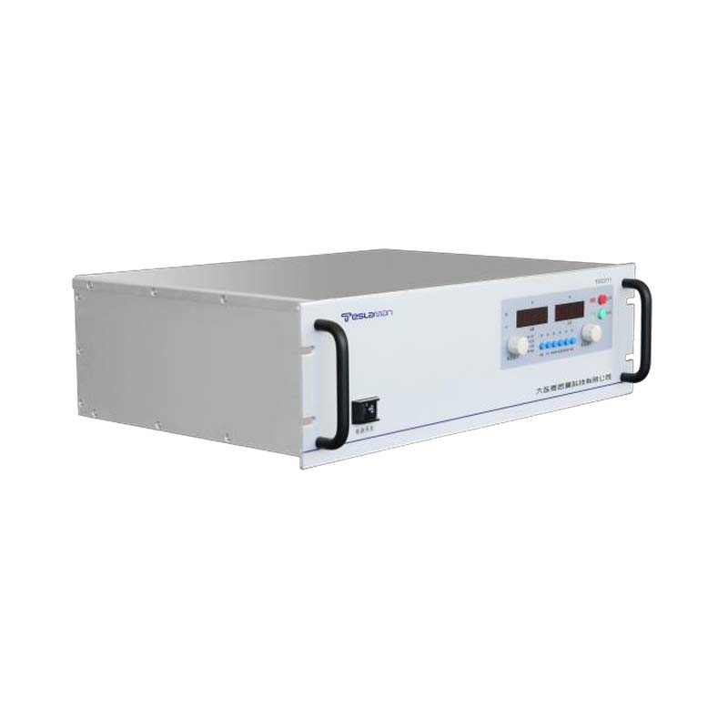
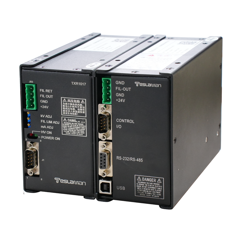
The power supply for this application must be capable of delivering a stable, controllable high voltage, often in the kilovolt range, at the elevated temperatures of the anneal. The wafer chuck must be designed to apply this voltage uniformly across the wafer while maintaining good thermal contact. This is a significant challenge, as the chuck materials must withstand both the high temperature and the high voltage. Ceramic materials with high thermal conductivity and high dielectric strength, such as aluminum nitride, are often used.
Furthermore, the process must be controlled to prevent arcing. At high temperatures, the air becomes more conductive, and the risk of a corona discharge or a full arc between the wafer and the surrounding electrodes increases. The high-voltage supply must have fast overcurrent protection to shut down in the event of an arc, and the chamber must be designed with adequate spacing and field grading to minimize the risk.
The benefits of synergistic annealing extend beyond defect passivation. The electric field can also enhance dopant activation. For some dopants, such as boron, the activation energy for moving from an interstitial to a substitutional site can be lowered by the presence of an electric field. This means that effective activation can be achieved at lower temperatures or in shorter times, reducing thermal budget and limiting diffusion.
Another promising application is in the annealing of compound semiconductors, such as gallium nitride. These materials are even more sensitive to damage from ion implantation, and their defects are often charged and mobile. Synergistic annealing with a high-voltage bias could provide a way to repair this damage without the extreme temperatures that can cause decomposition of the material.
The implementation of this technique requires a deep understanding of the physics of defects in semiconductors. The optimal voltage, the polarity, and the timing of the bias relative to the thermal cycle are all critical parameters that depend on the specific material, the implant conditions, and the desired device structure. This is a field where the high-voltage engineer must work closely with the process engineer and the device physicist to develop the right recipe.
In conclusion, high-voltage synergistic annealing represents a new dimension in semiconductor processing. By adding an electric field to the traditional thermal anneal, we gain an additional knob to control the behavior of defects and dopants. This allows for more effective defect passivation, higher dopant activation, and lower thermal budgets, all of which are essential for the continued scaling and performance improvement of semiconductor devices. The high-voltage power supply, in this context, is not just a source of energy but a precision tool for materials engineering at the atomic scale.